History of GaAsP LEDs
 26 февраля, 2014
  admin
admin The beginning of visible-spectrum LEDs dates back to the year 1962 when Holonyak and Bevacqua (1962) reported on the emission of coherent visible light from GaAsP junctions in the first volume of Applied Physics Letters. Although the emission of coherent light was only observed at low temperatures, the devices worked as LEDs and emitted visible light even at room temperature. This publication marks the beginning of viable p-n junction LEDs emitting in the visible wavelength range.
Nick Holonyak Jr., who in 1962 worked at General Electric in Syracuse, New York, and who later joined the University of Illinois, had used vapor-phase epitaxy (VPE) of GaAsP on GaAs substrates. This technique is suited for large-volume growth of wafers in a research as well as a manufacturing environment. Holonyak (2000) recalled that when he first had made these LEDs, he had already envisioned many applications these new devices might have, including indicator lights, seven-segment numeric displays, and alphanumeric displays.
However, despite the early success of the Holonyak group, the goal of demonstrating a semiconductor laser, working at room temperature, remained elusive (Holonyak, 1963, 1964). It remained elusive for good reasons. The GaAsP material system grown on GaAs substrates has several problems which Holonyak and co-workers discovered.
Although excellent electrical junction characteristics were obtained (Holonyak et al., 1963a), the optical properties degraded. When the phosphorus content in GaAsP was about 45-50%, a strong decrease in the LED radiative efficiency was found. These difficulties were attributed to the direct-indirect transition of the bandgap of GaAsP (Holonyak et al., 1963b, 1966; Pilkuhn and Rupprecht, 1964, 1965). It was determined that the 300 K efficiency of GaAsP alloy devices dropped to less than 0.005% when the phosphorus concentration exceeded 44% (Maruska and Pankove, 1967).
The first commercial GaAsP LED was offered by the General Electric (GE) Corporation in the early 1960s. The LED emitted visible radiation in the red part of the spectrum. The manufactured quantities of the product were low, probably due to the high price, which was 260 US$ for a single LED. The product was offered in the Allied Radio catalog, a widely distributed catalog for amateur radio electronics (Rostky, 1997).
The Monsanto Corporation was the first commercial entity to start mass production of LEDs. In 1968, the company had set up a factory, produced low-cost GaAsP LEDs, and sold them to
customers. The era of solid-state lamps had started. In the period 1968-1970, sales were skyrocketing, doubling every few months (Rostky, 1997). The Monsanto LEDs were based on GaAsP p-n junctions grown on GaAs substrates emitting in the visible red wavelength range (Herzog et al., 1969; Craford et al., 1972).
Monsanto developed a friendly collaboration with Hewlett-Packard (HP) Corporation, expecting that HP would make LEDs while Monsanto would provide the raw material - GaAsP. In the mid 1960s, Monsanto had sent one of its scientists from Saint Louis, Missouri, to Palo Alto, California, to help HP develop the LED business using Monsanto’s GaAsP material. However, HP felt nervous about depending on a single source for the GaAsP material. The informal relationship ended and HP started growing its own GaAsP (Rostky, 1997).
For several years, from the late 1960s to the mid 1970s, the emerging market was in numeric LED displays, driven at first by calculators, then by wristwatches, following Hamilton Watch Corporation’s introduction of the Pulsar digital watch in 1972. For a while, the early contenders, Monsanto and HP, took turns leaping into first place with a more advanced multiple-numeric or alphanumeric LED display (Rostky, 1997).
A key technical innovator and manager at Monsanto was M. George Craford, who has made numerous contributions to LEDs including the first demonstration of a yellow LED (Craford et al., 1972). It employed an N-doped GaAsP active region grown on a GaAs substrate. When Monsanto sold off its optoelectronics business in 1979, Craford joined HP and became the key person in the company’s LED business. A profile of Craford, who for many years served as Chief Technical Officer, was published by Perry (1995). In 1999, HP spun off parts of its business (including the LED business) into Agilent Corporation which in turn co-founded Lumileds Lighting Corporation in 1999, as a joint venture with Philips Corporation. In 2005, Agilent sold its share of Lumileds to Philips.
It soon became clear that the large lattice mismatch between the GaAs substrate and the GaAsP epilayer resulted in a high density of dislocations (Wolfe et al., 1965; Nuese et al., 1966). As a result, the external efficiency of these LEDs was quite low, about 0.2% or less (Isihamatsu and Okuno, 1989). The importance of the growth conditions and thickness of a buffer layer was realized by Nuese et al. (1969) who pointed out that a thick graded GaAsP buffer layer yields improved brightness red LEDs. It is understood today that the thick graded buffer layer reduces the high dislocation density in the GaAsP epitaxial layer originating near the GaAsP-epilayer-to - GaAs-substrate boundary.
The direct-indirect transitions as well as the high dislocation density limit the brightness attainable with GaAsP LEDs. Today this material system is primarily used for low-cost, lowbrightness red LEDs for indicator lamp applications.
1.1 History of GaP and GaAsP LEDs doped with optically active impurities Ralph Logan’s and his co-workers’ pioneering work on GaP LEDs was done while working at AT&T Bell Laboratories in Murray Hill, New Jersey, in the early 1960s, where they developed a manufacturing process for GaP-based red and green LEDs. At that time, semiconductors had been employed to demonstrate both bipolar and field-effect transistors for switching and amplifying electrical currents. Engineers and scientists back then also began to realize that semiconductors would be perfectly suitable for light-emitting devices.
Logan (2000) recalls that his interest was stimulated by the first reports of GaP p-n junction LEDs by Allen et al. (1963) and Grimmeiss and Scholz (1964). Theses devices emitted red light at a useful efficiency so that the light could be clearly seen with the naked eye under ambient daylight conditions. The Grimmeiss-Scholz junctions had been reported to be made by alloying Sn, an n-type dopant, into p-type GaP.
|
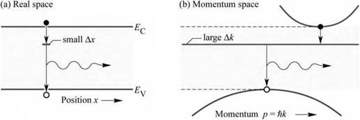
Fig. 1.5. (a) Real-space and (b) momentum-space optical transitions in GaP doped with an optically active impurity such as О or N, emitting in the red and green parts of the spectrum, respectively. GaP LEDs employ the uncertainty principle (ДxAp > И/2k) which predicts that an electron wave function localized in real space is delocalized in momentum space, thereby making momentum-conserving (vertical) transitions possible. |
GaP is an indirect-gap semiconductor that does not emit significant amounts of light due to the requirement of momentum conservation in optical transitions. Figure 1.5 shows the band diagram of GaP illustrating that the band extremum points occur at different values in momentum space. If GaP is doped with an optically active isoelectronic impurity such as N, strong optical transitions are obtained, as shown by Thomas et al. (1965), because the impurity levels are smeared out in momentum space. GaP doped with optically active impurities is a wonderful example of a practical device based on the Heisenberg uncertainty principle, which predicts that an impurity with a strongly localized wavefunction in position space (small Ax) will have a delocalized level in momentum space (large Ak), so that optical transitions can occur via the deep-level state.
The growth of GaP was accomplished by using platelets grown from a solution containing Ga and P. The platelets had lateral dimensions of 0.5 cm x 1 cm and were grown to a thickness of about 1 mm. This was the standard initial method of growing GaP and overcame the problem of dealing with the P overpressure required when growing GaP at high temperatures. No one at Bell Laboratories could immediately reproduce the remarkable results reported by Grimmeiss and Scholz. However, a big research effort in electroluminescence was launched at Bell Laboratories as a result.
In the solution growth of the GaP platelets, the dopants used were Zn and O (the latter from Ga2O3), but it was not generally realized that ordinary ambient air usually contains enough S to be a good n-dopant. The growth kinetics of the platelets had the intriguing result that the compensated melts generally produced an n-type layer on one platelet surface so that a p-n junction was formed under the GaP platelet surface. This was thought to explain Grimmeiss’ results. Logan et al. (1967a) published these findings at once.
Logan’s research group also reported the first demonstration of reproducible growth of efficient LEDs (Logan et al., 1967b). These junctions were formed by growing an n-type GaP layer onto Zn-O-doped GaP wafers that were polished out of large solution-grown wafers with typical sizes of 2.5 x 2.5 cm2. Logan et al. found that post-growth annealing in the range 400725 °C could increase the LED efficiency by as much as an order of magnitude, yielding efficiencies exceeding 2%. The annealing was thought to diffuse the Zn to the O atoms, thereby increasing the density of isoelectronic Zn-O centers that mediated the electroluminescence.
At the end of the 1960s, ingots of GaP grown from melts at high temperature and pressure were becoming available, suitable for being cut into real substrates as we know them today. Green LEDs were formed with efficiencies as high as 0.6% by doping the GaP with N isoelectronic impurities (Logan et al., 1968, 1971). The N was added in the form of GaN to the growth melts used to form the p-n junctions. While the external quantum efficiency of green LEDs is less than for the red LEDs, the sensitivity of the human eye to green light is more than 10 times higher than in the red, so the apparent brightness of the LEDs is comparable.
Other research laboratories such as IBM, RCA, and GE also looked into the possibility of making visible-spectrum LEDs that were more efficient than those made of GaAsP. Research on
|
И Substrate contact Д |
|
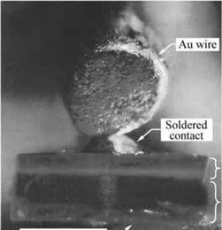
Fig. 1.6. GaP light-emitting diode grown by liquid-phase epitaxy emitting “brilliant red light” from the Zn - and O-doped p-n junction region (courtesy of Pilkuhn, 2000). n-GaP epilayer p-GaP substrate |
|
The active regions of Pilkuhn’s GaP LEDs were co-doped with acceptors, e. g. Zn acceptors, and donors, e. g. Te, S, or Se donors, so that light was generated predominantly by donor - acceptor pair recombination processes. The energy of the light was below the bandgap of GaP. It was also found that co-doping of GaP with Zn and O resulted in a particularly large wavelength shift so that the emission occurred in the red wavelength range (Foster and Pilkuhn, 1965). Oxygen in GaP is neither donor nor acceptor but was identified as a deep level (see, for example, Pilkuhn, 1981). Logan and co-workers, and their management team at AT&T Bell Laboratories immediately realized that there were many possible applications for LEDs. Indicator lamps were becoming useful in the telephone business. All such lights used at that time in the USA operated using 110 V. An example is the “Princess” telephone, which was intended to be used in bedrooms - the dial lit up when the phone was picked up from its cradle. The “Princess” was a prestigious telephone and the latest fad in the 1960s but had to be installed near a 110 V outlet. A service call to the local phone company was needed if the bulb burned out. If LEDs were to replace the |
GaP LEDs was pursued at IBM Corporation’s Thomas J. Watson Research Center in Yorktown Heights in New York State. Manfred Pilkuhn and co-workers demonstrated an LPE-grown red GaP LED doped with Zn and O. The picture of a GaP LED with top and bottom contacts is shown in Fig. 1.6. The IBM Research Journal proudly reported that “brilliant red light” was emitted from the p-n junction. Note that in the 1960s, monochromatic colors were mostly generated by filtering incandescent light, so that the narrow-spectral-width LED light appeared to the observer as an impressively pure and “brilliant” color.
110 V light bulbs, the phone line could power the LEDs and a 110 V outlet would no longer be needed. In addition, GaP LEDs had an expected lifetime exceeding 50 years when used in telephones, much longer than 110 V light bulbs, so that this reliability promised substantial cost savings for the “Bell System” or simply “Ma Bell”, as the phone company was called at that time.
More important was the multi-line “key telephone”. This is the multi-line telephone used in large offices mostly by operators and secretaries where indicator lamps tell which line is being called and busy. To switch the telephone lines and the 110 V indicator lamps, a remote switch was used with dozens of wires to each phone. Installing and servicing these phones was very costly. In present-day telephones, the LED indicator lamps are powered over the phone line. A compatible circuit inside the phone handles the switching of the indicator lamps and phone lines. The savings in telephone manufacturing, installation, and service were impressive.
With the demonstration of the reproducible growth of efficient green N-doped GaP LEDs and red Zn-O-codoped LEDs, both of which were about equally bright and useful, the Bell Laboratories Development Department decided to manufacture the LEDs at its Reading, Pennsylvania, facility.
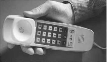
Telephone lines typically operate with a line voltage of approximately 40 V DC with currents of several milliamperes. The only effect of inserting an LED into this circuit is to reduce the drive voltage by approximately 2 V, a negligible effect, while the efficient LED makes a good indicator lamp. As a result, many phone models were equipped with an illuminated dial pad. Both red and green LED illumination was available, and green was the final choice made by telephone designers. Figure 1.7 shows a 1990 version of the AT&T Trimline telephone - still using GaP:N green LEDs for the dial pad illumination. Red and green LEDs were also incorporated in the multi-line “key telephones”.
Should the reader ever be near Murray Hill, New Jersey, visiting the Bell Laboratories Museum, located at 600 Mountain Avenue, should be considered. Many technical artifacts including Logan et al.’s green GaP:N LED are displayed in the museum.
The Monsanto team applied N doping to GaAsP to attain emission in the red, orange, yellow, and green wavelength range (Groves et al., 1971; Craford et al., 1972; for a review see Duke and Holonyak, 1973). Many parameters, such as the emission and the absorption wavelength and the solubility of N in GaAsP and GaP were investigated. A useful growth method was vapor-phase epitaxy (VPE), because it allowed for N-doping in the vicinity of the p-n junction only. This resulted in less absorption of light in the layers adjoining the p-n junction and higher overall
LED efficiencies (Groves et al., 1977, 1978a, 1978b). Today, GaP:N is the primary material for green emitters used in low-brightness applications such as indicator lights.
|
|
|
Fig. 1.7. AT&T telephone set (“Trimline” model) with the dial pad illuminated by two green N-doped GaP LEDs. The illuminated dial pad was one of the first applications of green GaP:N LEDs. |
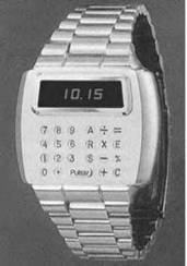
The first digital wristwatch with an LED display was released in 1972 by the Hamilton watch company. The watch became an instant furor and only its high price prevented it from becoming widely distributed. The digital Pulsar watch with an integrated calculator was released in 1975 and is shown in Fig. 1.8.
|
|
|
Fig. 1.8. Pulsar calculator watch with LED display released in 1975 by Hamilton Corporation. The first Pulsar LED watch (without calculator) was offered in 1972. It was based on GalnP LEDs (after Seiko, 2004). |
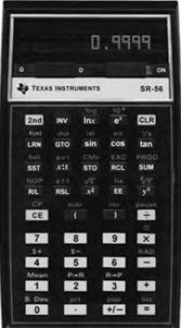
Another early application of LEDs was the numeric display in pocket calculators. Figure 1.9 shows two programmable calculators of the mid 1970s, the Texas Instruments Corporation’s SR - 56 and the Hewlett-Packard Corporation’s HP-67. Both used red GaAsP LEDs in the seven - segment numeric display. All calculators using LED displays shared a significant problem: the display could not be read under bright outdoor conditions because the light emitted by the LEDs was simply too dim; furthermore, the power consumption of LED displays was high so that the rechargeable battery running the calculator had to be recharged on a regular basis. Digital wrist
watches using LEDs shared the same problem. Liquid crystal displays (LCDs), introduced at the end of the 1970s, had much lower power requirements. Consequently, LCDs totally replaced LED displays in calculators and watches by the beginning of the 1980s.

|
x*o Xty |
8•**' |
COS-' |
w* |
|
*! |
n |
0 |
ШМ |
|
x<0 x$y |
RSP |
or R |
H ГНМ8 |
|
Щ |
199 |
я |
■__ J |
|
*>0 x>y |
X XCH |
INT FRAC |
-X - STK |
|
|
|
Fig. 1.9. Programmable pocket calculators Model SR-56 of the Texas Instruments Corporation and Model HP-67 of the Hewlett-Packard Corporation, both first manufactured in 1976. Seven-segment numeric characters composed of GaAsP LEDs were used in the display. The SR-56 came with a “huge” program memory of 100 steps. The HP-67 came with a magnetic card reader and had several freely programmable keys. |
|
abed* HI. ИД у. ЙІіі, ДЯц * ■ 088 f ИХ 80 R*0 LBLf |
|
■ У! Щ " I 08Z Ш I8Z (I) ччч W/DATA MERGE P*8 CL RCO ClPROM
|
1.2 History of GaN metal-semiconductor emitters
In the late 1960s, the Radio Corporation of America (RCA) was one of the premier manufacturers of color televisions, using cathode ray tubes (CRT) with three electron guns to display images. At RCA’s central research laboratory in Princeton, New Jersey, James Tietjen had become the director of the Materials Research Division, and he wanted to develop a flat - panel television display that could be hung on the wall like a painting. To create a full color image, the display must contain red, green, and blue pixels. Tietjen realized that red LEDs using GaAsP and green LEDs using GaP:N technology were already available. All that was needed for a flat TV based on LEDs was a bright blue LED.
In May 1968, Tietjen approached a young man in his group, Paul Maruska, and challenged him to find a method for growing single-crystal films of GaN, which Tietjen felt would yield blue LEDs. Maruska had been growing GaAsP red LEDs using the metal-halide vapor-phase epitaxy (MHVPE) approach. He gained much experience with the promises and perils of III-V compounds including phosphorus, a pyrophoric substance. On a day in 1968, phosphorus caused a garbage truck to catch fire on New Jersey’s Route 1 in Princeton shortly after picking up some
phosphorus-containing laboratory waste at the RCA Laboratories. The driver of the truck decided to immediately return the burning and smoking load to RCA and dump it on the front lawn of the research laboratories (Maruska, 2000).
When Maruska started working on GaN, he first went to the library at Princeton University and thoroughly studied copies of all the old papers on GaN from the 1930s and 1940s (Juza and Hahn, 1938). GaN had been prepared as a powder by reacting ammonia with liquid gallium metal at elevated temperatures. He chose sapphire as the substrate because it is a robust material that is not reactive with ammonia. Unfortunately, he misinterpreted the results of Lorenz and Binkowski (1962), who had reported the decomposition of GaN in vacuum at temperatures as low as 600 °C. All of his early GaN films were grown at temperatures below 600 °C to prevent decomposition, and hence were polycrystalline. Finally in March 1969, Maruska realized that in an ammonia environment, growth rather than decomposition would occur, and thus he raised the furnace temperature to 850 °C, the temperature typically used for GaAs growth. The sapphire appeared to be uncoated, because the GaN film was clear and had a specular surface. He rushed down to the RCA analytical center, and a Laue pattern revealed that the deposit was indeed the first single-crystal film of GaN (Maruska and Tietjen, 1969).
Maruska found that all of the GaN films were n-type without intentional doping. He sought to find a p-type dopant so that he could make a p-n junction. Zinc seemed to be an appropriate acceptor because it worked for GaAs and GaP. With heavy Zn concentrations, GaN films proved to be insulating. But they were never conducting p-type (Maruska, 2000).
During 1969, Jacques Pankove spent a sabbatical year at Berkeley University writing his classic textbook, Optical Processes in Semiconductors. When he returned to RCA Laboratories in January 1970, he immediately became interested and strongly involved in the new GaN films. Pankove et al. undertook a study of optical absorption and photoluminescence of thin-film GaN (Pankove et al., 1970a, 1970b). The first example of electroluminescence from GaN was announced at RCA in the summer of 1971 (Pankove et al. 1971a). The sample consisted of an insulating Zn-doped layer which was contacted with two surface probes, and blue light centered at 475 nm was emitted. Pankove and co-workers then made a device consisting of an undoped n - type region, an insulating Zn-doped layer, and an indium surface contact (Pankove et al., 1971b, 1972). This metal—insulator—semiconductor (MIS) diode was the first current-injected GaN light emitter, and it emitted green and blue light.
The RCA team speculated that magnesium might be a better choice of p-type dopant than zinc. They began growing Mg-doped GaN films using the MHVPE technique, and in July 1972,
obtained blue and violet emission centered at 430 nm as shown in Fig. 1.10 (Maruska et al., 1972). One of these Mg-doped blue light MIS emitters continues to emit light even today. Maruska et al. (1973) described these efforts in a paper entitled “Violet luminescence of Mg - doped GaN”. Note that the GaN films, even though Mg doped, did not exhibit p-type conductivity, so that the luminescence in these films was probably mediated by minority carrier injection or impact ionization in the high-field insulating regions of the films. Pankove and the RCA team offered a model for the operation of these devices based on impact ionization and Fowler-Nordheim tunneling, because the characteristics were virtually independent of temperature (Pankove and Lampert, 1974; Maruska et al., 1974a, 1974b). Of course, these devices were inefficient, and as a consequence, Tietjen, who had stimulated the work, now terminated it by ordering “stop this garbage” - words that Maruska (2000) still vividly remembers.
|
|
Fig. 1.10. Blue light emission found in 1972 caused by recombining electron-hole pairs created in a highly resistive GaN structure doped with Si and Mg (courtesy of Maruska, 2000).



 Опубликовано в