Visible-spectrum LEDs
 28 марта, 2014
  admin
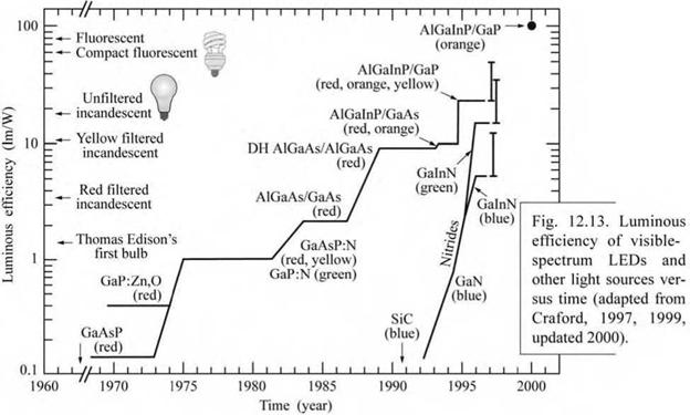
admin Originally, LEDs were exclusively used for low-brightness applications such as indicator lamps. In these applications, the efficiency and the overall optical power of the LED are not of primary importance. However, in more recent applications, for example traffic light applications, the light emitted by LEDs must be seen even in bright sunlight and from a considerable distance. LEDs with high efficiency and brightness are required for such applications.
In this chapter, low-brightness as well as high-brightness LEDs are discussed. GaAsP and nitrogen-doped GaAsP LEDs are suitable only for low-brightness applications. AlGaAs LEDs are suitable for low - as well as high-brightness applications. AlGaInP and GaInN LEDs are used in high-brightness applications.
12.1 The GaAsP, GaP, GaAsP:N, and GaP:N material systems The GaAs1-xPx and GaAs1-xPx:N material system is used for emission in the red, orange, yellow, and green wavelength range. The GaAsP system is lattice mismatched to GaAs substrates, resulting in a relatively low internal quantum efficiency. As a result these LEDs are suitable for low-brightness applications only.
GaAs1-xPx was one of the first material systems used for visible-spectrum LEDs (Holonyak and Bevacqua 1962; Holonyak et al. 1963, 1966; Pilkuhn and Rupprecht 1965; Wolfe et al., 1965; Nuese et al. 1966). In the early 1960s, GaAs substrates were already available. Bulk growth of GaAs substrates was initiated in the 1950s and epitaxial growth by LPE and VPE started in the 1960s. As phosphorus is added to GaAs, the ternary alloy GaAs1-xPx, or briefly GaAsP, is formed. The addition of phosphorus increases the bandgap of GaAs, which emits in the infrared at 870 nm. The visible wavelength range starts at about 750 nm, so that a small amount of phosphorus is sufficient to attain visible-spectrum light emitters. Note, however, that the sensitivity of the human eye is low at the edges of the visible spectrum.
A significant problem with GaAsP LEDs is the lattice mismatch between the GaAs substrate and the GaAsP epitaxial layer. A large mismatch exists between GaAs and GaP (about 3.6%) so that many misfit dislocations occur when the critical thickness of GaAsP on GaAs is exceeded. As a result, the luminescence efficiency decreases substantially in GaAsP with increasing phosphorus content. GaAsP LEDs are therefore useful for low-brightness applications only.
It was realized early in the GaAsP work that the lattice mismatch between the GaAs substrate and the GaAsP epilayer reduces the radiative efficiency. It was also found that the radiative efficiency of the active p-n junction layer strongly depends on the growth conditions and, in particular, on the thickness of the GaAsP buffer layer (Nuese et al., 1969). A thick buffer layer reduces the dislocation density by annihilation of misfit dislocations. However, the dislocation density does not approach the low dislocation density of GaAs substrates, so that even with thick GaAsP buffer layers the dislocation density is substantial.
The band structure of GaAs, GaAsP, and GaP is shown schematically in Fig. 12.1. The figure shows that GaAsP is a direct-gap semiconductor for low phosphorus mole fractions. Beyond the direct-indirect crossover occurring at phosphorus mole fractions of about 45-50%, the semiconductor becomes indirect and the radiative efficiency drops rapidly (Holonyak et al., 1963, 1966). GaP is an indirect-gap semiconductor and therefore is unsuitable as an efficient LED material.
GaAsP and GaP LEDs are frequently doped with isoelectronic impurities such as nitrogen (Grimmeiss and Scholz, 1964; Logan et al., 1967a, 1967b, 1971; Craford et al., 1972; Groves and Epstein 1977; Groves et al. 1978a, 1978b). The isoelectronic impurities form an optically active level within the forbidden gap of the semiconductor so that carriers recombine radiatively via the nitrogen levels, as indicated in Fig. 12.1.
|
(a) Direct-gap GaAs (b) Crossover GaAs0 cqPq (c) Indirect-gap GaP
Fig. 12.1. Schematic band structure of GaAs, GaAsP, and GaP. Also shown is the nitrogen level. At a P mole fraction of 45—50%, the direct—indirect crossover occurs. |
Isoelectronically doped LEDs are also interesting from a fundamental point of view. They are one of the first practical applications of Heisenberg’s uncertainty principle. Isoelectronic impurities have an electronic wave function that is strongly localized in position space (small Ax). Therefore, the wave function is delocalized in momentum space (large Ap). Since the level is delocalized in momentum space, two vertical transitions can occur via the isoelectronic trap, with one of them being radiative. Physically speaking, the change in momentum, occurring when an electron makes a transition from the indirect X valley of the conduction band to the central Г valley of the valence band, is absorbed by the isoelectronic impurity atom.
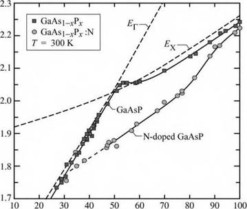
The emission wavelength of undoped and nitrogen-doped GaAsP is shown in Fig. 12.2 (Craford et al., 1972). The emission energy of GaAsP and GaP doped with the isoelectronic impurity nitrogen is below the bandgap of the semiconductor. Figure 12.2 illustrates that the emission energy is about 50-150 meV below the bandgap of the semiconductor. As a result, reabsorption effects are much less likely in nitrogen-doped structures compared with LEDs based on band-edge emission. This is a substantial advantage of LEDs doped with isoelectronic impurities.
|
|
|
Fig. 12.2. Room-temperature peak emission energy versus alloy composition for undoped and nitrogen-doped GaAsP LEDs injected with a current density of 5 A/ctrr. Also shown is the energy gap of the direct - to-indirect (£r-to-£x) transi‘ tion. The direct—indirect crossover occurs at л: = 50% (after Craford et a!., 1972). |
|
Phosphorus mole fraction. v (%) |
Groves et al. (1978a, 1978b) showed that this advantage is particularly pronounced if only the active region is doped with nitrogen. In this case, the region of the p-n junction plane and the regions located within the carrier diffusion lengths from the junction plane are doped with nitrogen. Other regions, such as the confinement and window layers, are not doped with the isoelectronic impurity, so that reabsorption of light by the isoelectronic impurities is limited to the narrow active region. Quantum efficiencies of several percent can be attained with GaP:N LEDs in which the nitrogen doping is limited to the active region.
|
|
|
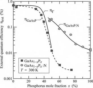
Fig. 12.3. Experimental external quantum efficiency of undoped and N-doped GaAsP versus the P mole fraction. Also shown is the calculated direct-gap (Г) transition efficiency, r)p, and the calculated nitrogen (N) related transition efficiency, r|xj (solid lines). Note that the nitrogen-related efficiency is higher than the direct-gap efficiency in the indirect bandgap (x > 50%) regime (after Campbell el al., 1974). |
The external quantum efficiency of undoped and nitrogen-doped GaAsP is shown in Fig. 12.3 (Campbell, 1974). Only the vicinity of the active region is doped with nitrogen. The efficiency of the nitrogen-doped LEDs is strongly enhanced over the entire composition range compared with the GaAsP LEDs without nitrogen doping.
Note that the GaAsP LED efficiency decreases by more than two orders of magnitude in the composition range x = 40-60%. This decrease is due to the direct-indirect crossover occurring in GaAsP and due to the increasing dislocation density occurring at higher phosphorus mole fractions. At a phosphorus mole fraction of 75%, the GaAsP external quantum efficiency is only 0.002%.
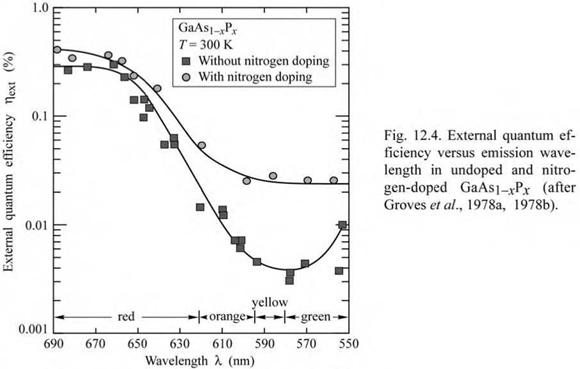
The external quantum efficiency of undoped and nitrogen-doped GaAsP versus emission wavelength is shown in Fig. 12.4. Again, only the vicinity of the active region is doped with nitrogen. The efficiency of nitrogen-doped GaAsP is higher than that of undoped GaAsP, in particular in the orange, yellow, and green wavelength range where the improvement is a factor of 2-5. In the red wavelength range, the undoped and nitrogen-doped GaAsP LEDs have similar efficiencies.
|
|
The ratio of external quantum efficiencies of undoped and nitrogen-doped GaAsP LEDs is shown in Fig. 12.5. It is inferred from the figure that nitrogen-doped devices have a higher efficiency over the entire composition range.
|
< a < я о о га к>> о с ■ У <3 £ |
|
100 |
25
|
1 1 1 GaAsl-.vPx:N and GaAs |_XPV _ T = 300 К |
|
|
- |
- |
|
- |
. - |
|
1 I 1 |
o “ 1 I I |
|
20 |
|
15 |
|
10 |
|
30 40 50 60 70 80 90 Phosphorus mole fraction x (%) |
Fig. 12.5. Efficiency ratio between nitrogen-doped and undoped GaAsi-xP* at 300 К (after Groves et al., 1978a, 1978b).
The brightness of LEDs based on isoelectronic impurity transitions is limited by the finite solubility of nitrogen. For example, nitrogen is soluble in GaP up to nitrogen concentrations of
about 1020 cm-3. Since an optical transition via a nitrogen level has a certain lifetime, the maximum nitrogen concentration limits the LED operation to a maximum current beyond which the LED efficiency decreases.
Commercial low-brightness green LEDs are based on nitrogen-doped GaP. The main application of GaP:N LEDs is indicator lamps. However, nitrogen-doped GaP LEDs are not suitable for high-brightness applications, i. e. for applications under bright ambient light conditions such as sunlight. High-brightness green LEDs are based on GaInN.
|
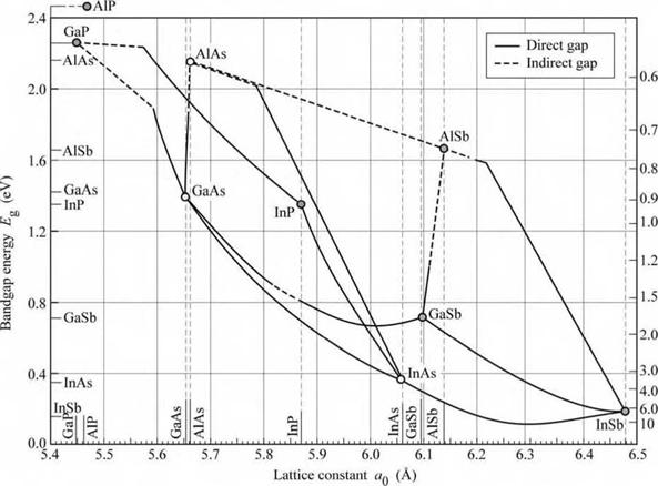
Fig. 12.6. Bandgap energy and lattice constant of various III—V semiconductors at room temperature (after Tien, 1988). |
12.2 The AlGaAs/GaAs material system The AlxGa1-xAs/GaAs material system was developed in the 1970s and early 1980s and it was the first material system suitable for high-brightness LED applications (for a review, see Steranka, 1997). Owing to the very similar atomic radii of Al (1.82 A) and Ga (1.81 A), the material system AlxGa1-xAs (or briefly AlGaAs) is lattice matched to GaAs for all Al mole
fractions. The lack of dependence of the lattice constant on the Al mole fraction can be inferred from Fig. 12.6, which shows the energy gap and lattice constant of several III-V semiconductors and of its ternary and quaternary alloys as a function of the lattice constant (adopted from Tien, 1988).
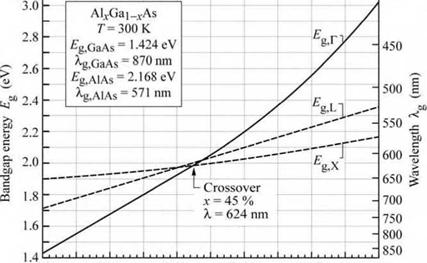
GaAs and AlxGa1-xAs for Al mole fractions x < 0.45 are direct-gap semiconductors. The energy gap of AlxGa1-xAs versus the Al mole fraction is shown in Fig. 12.7 (Casey and Panish, 1978). For Al mole fractions x < 45%, the Г conduction-band valley is the lowest minimum and the semiconductor has a direct gap. For x > 45%, the X valleys are the lowest conduction-band minimum and the semiconductor becomes indirect.
|
|
|
Egj/cV= 1.424+ 1.247 л: '___________________ (0 <дг < 0.45) £gj-/eV= 1.424+ 1.247л: + 1.147(x-0.45) (0.45 <x< 1.0) £g, L/eV= 1.708+ 0.642* ’___________ (0 <лг< 1.0) £g, x /eV= 1.900 + 0.125 Л - + 0.143 Xі (0<*<1.0) |
|
Fig. 12.7. Bandgap energy and emission wavelength of AlGaAs at room temperature. Ey denotes the direct gap at the Г point and EL and Ex denote the indirect gap at the L and X point of the Brillouin zone, respectively (adapted from Casey and Panish, 1978). |
|
»і 11jі 11»j11 11 1111 іjі і і іjі і і іj11»іj і 11»j і і і і j і і і і 400 |
|
0.0 0.20 0.40 0.60 0.80 1.0 |
|
GaAs AlvGa| As alloy composition л: (-) AlAs |
The AlGaAs material system is suited for high-brightness visible-spectrum LEDs emitting in the red wavelength range. The direct-indirect crossover occurs at a wavelength of 621 nm. At that wavelength, the radiative efficiency of the AlGaAs system becomes quite low due to the direct-indirect transition. To maintain high efficiency, the emission energy must be several kT lower than the bandgap energy at the direct-indirect crossover point.
There are several possible strategies for AlGaAs-based red LEDs, including AlxGa1-xAs bulk active regions, AlxGa1-xAs/GaAs quantum well active regions, and AlxGa1-xAs/AlyGa1-yAs (x > y) double heterostructure active regions. The first possibility, AlxGa1-xAs bulk active regions, lacks the advantages of a heterostructure and this approach is therefore not used in highbrightness LEDs. The two other possibilities are more attractive due to the employment of
heterostructures. The quantum well and double heterostructure active region is used in high - efficiency red LEDs and the two structures are shown schematically in Fig. 12.8. In the AlxGa1-x As/GaAs quantum well case shown in Fig. 12.8 (a), size quantization is used to increase the emission energy. In the case of the AlxGa1-xAs/Al^Ga1-yAs double heterostructures shown in Fig. 12.8 (b), AlGaAs is used for both the barrier region and the well region. A drawback of the AlxGa1-xAs/GaAs quantum well active regions is the requirement of very thin GaAs quantum wells clad by AlxGa1-xAs barriers. Vertical transport in multi-quantum well (MQW) structures can lead to non-uniform carrier distribution in the MQW active region unless the barriers are very thin. Consequently, the AlxGa1_xAs/Al_vGa1_yAs double heterostructure approach is usually preferred.
|
AlvGa|_xAs |
(a) AlvGa)_xAs/GaAs QW structure (b) AlvGa|_д-As/A1 ,.Ga]_VAs DH structure
AlvGa|_vAs AlvGa|_vAs AIvGa|_xAs
GaAs AlvGa|_vAs (x > д>)
Fig. 12.8. Band diagrams of AlGaAs/GaAs structures suited for emission in the red part of the visible spectrum, (a) AlGaAs/GaAs quantum well (QW) structure with a thin GaAs well, (b) AlGaAs/AlGaAs double heterostructure (DH) with an AlGaAs active region.
AlGaAs/GaAs LEDs have been fabricated as homostructures, single heterostructures, and double heterostructures (Nishizawa et al., 1983). The most efficient AlGaAs red LEDs are double-heterostructure transparent-substrate (DH-TS) devices (Ishiguro et al., 1983; Steranka et al. 1988; Ishimatsu and Okuno, 1989). AlGaAs DH-TS LEDs are grown on temporary GaAs substrates and consist of a thick (e. g. 125 ^m) AlxGa1-xAs lower confinement layer with an Al mole fraction x > 60%, an AlxGa1-xAs active layer (x = 35%, for red devices), and a thick (e. g. 125 |jm) AlxGa1-xAs upper confinement layer, also with an Al mole fraction x > 60%. For devices emitting in the IR, the Al mole fractions of the active and confinement layers can be lower. After epitaxial growth, the absorbing GaAs substrate is removed by polishing and selective wet chemical etching. AlGaAs DH-TS LEDs are more than a factor of 2 brighter than double-heterostructure absorbing-substrate (DH-AS) devices (Steranka et al., 1988).
In the 1980s the growth method of choice for AlGaAs DH-TS LEDs was liquid-phase epitaxy (LPE). This growth method is capable of growing, at a high growth rate, very thick high - quality AlGaAs layers with high Al content. LPE can be scaled up for high-volume production
(Ishiguro et al., 1983; Steranka et al., 1988; Ishimatsu and Okuno, 1989). AlGaAs/GaAs DH-AS LEDs have also been grown by OMVPE (Bradley et al., 1986). However, the OMVPE growth rate is lower than the LPE growth rate. OMVPE growth of thick layers, as required for DH-TS devices, is therefore difficult. Historically AlGaAs DH-TS LEDs were the first high-brightness LEDs suitable for demanding applications such as automotive brake lights and traffic lights, which must be clearly visible under bright ambient conditions.
The reliability of AlGaAs devices is known to be lower than that of AlGaInP devices that do not contain any AlGaAs. High-Al-content AlGaAs layers are subject to oxidation and corrosion, thereby lowering the device lifetime. Dallesasse et al. (1990) reported the deterioration of AlGaAs/GaAs heterostructures by hydrolysis. Cracks, fissures, and pinholes were found after long-term exposure to room environmental conditions, especially for thick AlGaAs layers (> 0.1 цш) with a high Al content such as 85%. The authors found very thin AlGaAs layers (e. g. 20 nm) to be stable, even for Al contents of 100%. Hermetic packaging is required to avoid oxidation and hydrolysis of AlGaAs layers. Steranka et al. (1988) stated that some AlGaAs devices on the market have exhibited severe degradation. However, accelerated aging data taken at 55 °C with an injection current of 30 mA showed no degradation at all after 1000 h of stress. Such a performance requires excellent understanding and control of the device fabrication and packaging process.
12.3 The AlGaInP/GaAs material system The AlGaInP material system was developed in the late 1980s and early 1990s and today is the primary material system for high-brightness LEDs emitting in the long-wavelength part of the visible spectrum, i. e. in the red, orange, amber, and yellow wavelength range. The AlGaInP material system and AlGaInP LEDs have been reviewed by Stringfellow and Craford (1997), Chen et al. (1997), and Kish and Fletcher (1997). Further reviews and recent developments were published by Mueller (1999, 2000) and Krames et al. (2002).
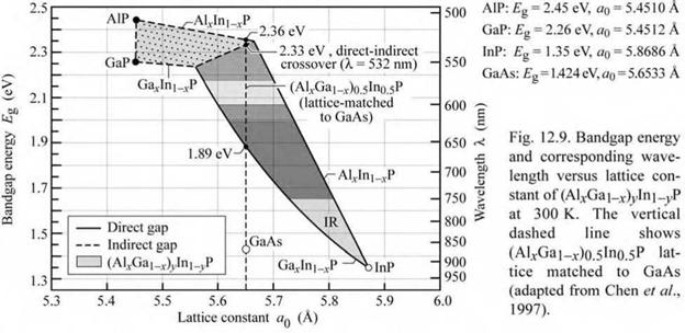
Figure 12.9 shows the energy gap and the corresponding wavelength versus the lattice constant of AlGaInP (Chen et al., 1997). AlGaInP can be lattice matched to GaAs. Replacing all As atoms in the GaAs lattice by smaller P atoms and some of the Ga atoms in the GaAs lattice by larger In atoms, forms GaInP, which at the particular composition Ga05In05P, is lattice matched to GaAs. Since Al and Ga have very similar atomic radii, the material (AlxGa1-x)05In05P is also lattice matched to GaAs.
|
|
|
у с с. я SIl — с а CQ |
|
I |
|
1.8 |
2.6
|
<Л1лОаІ-л-)0.5ІП |
0.5P |
||||||||
|
T= Er |
300 к = 1.91 eV + 0.61 e V x л* |
||||||||
|
4 |
= 2.19 eV + 0.085 eVxx |
||||||||
|
*-Cr |
OSSOY4 53 % = 555 |
T |
Lx |
- |
|||||
|
Er^ |
X'- |
im |
- |
||||||
|
- |
|||||||||
|
.... |
.... |
.... |
. . . . 1 |
. . . . 1 |
.... |
.... |
.... |
.... |
.... |
|
2.4 |
|
2.2 |
|
2.0 |
|
0.0 0.20 0.40 0.60 0.80 (Al Ga. )0 sIn0 5P alloy composition x (-) |
|
Я 480 500 520 540 |
|
560 І 580 I 600 « 620 640 660 680 1.0 |
Fig. 12.10. Bandgap energy and emission wavelength of unordered AlGaInP lattice matched to GaAs at room temperature. Er denotes the direct gap at the Г point and denotes the indirect gap at the X point of the Brill - ouin zone (after Prins et al., 1995 and Kish and Fletcher, 1997).
According to Chen et al. (1997), (AlxGa1-x)05In05P has a direct bandgap for x < 0.5 and an indirect bandgap for x > 0.5. At the crossover point (x = 0.5), the bandgap energy is 2.33 eV, corresponding to a wavelength of 532 nm. Kish and Fletcher (1997) compiled data from Prins et al. (1995) and concluded that (AlxGa1-x)05In05P is a direct-gap semiconductor for Al mole fractions x < 0.53. The energy gap versus Al mole fraction is shown in Fig. 12.10 (Prins et al., 1995; Kish and Fletcher, 1997). At Al mole fractions x < 53%, the Г conduction-band valley is the lowest minimum and the semiconductor has a direct gap. For x > 53%, the X valleys are the lowest conduction-band minimum and the semiconductor becomes indirect. The emission wavelength at the direct-indirect crossover point is approximately 555 nm. The exact
wavelength of the crossover point may depend on the degree of atomic ordering present in a particular material (Kish and Fletcher, 1997).
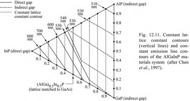
A contour plot of the lattice constant and the energy gap of the AlGaInP materials system is shown in Fig. 12.11 (Chen et al., 1997). The bandgap energy values and the composition of the direct-indirect crossover shown in Fig. 12.11 are slightly different from the data shown in Fig. 12.10, which can be attributed to atomic ordering in AlGaInP. Atomic ordering lowers the bandgap energy by values up to 190 meV (Kish and Fletcher, 1997).
|
|
The AlGaInP material system is suited for high-brightness visible-spectrum LEDs emitting in the red, orange, amber, and yellow wavelength range. At the direct-indirect crossover the radiative efficiency of the AlGaInP system is quite low due to the direct-indirect transition. To maintain high efficiency, the emission energy should be several kT lower than the bandgap energy at the direct-indirect crossover point.
12.4 The GaInN material system The GaInN material system was developed in the early 1990s. GaInN LEDs emitting in the blue and green wavelength range became commercially available in the late 1990s. To date GaInN is the primary material system for high-brightness blue and green LEDs. The GaInN material system and GaInN LEDs have been reviewed by Nakamura and Fasol (1997) and by Strite and Morkoc (1992).
One of the greatest surprises of the GaInN materials system is its high radiative efficiency despite the presence of a very high concentration of threading dislocations in GaInN/GaN epitaxial films. These threading dislocations are due to the lattice mismatch between the commonly used sapphire and SiC substrates and the GaN and GaInN epitaxial films. Typical densities of the threading dislocations are in the 107-109 cm-2 range.
In the III-V arsenide and III-V phosphide material systems, misfit dislocations have disastrous consequences for the radiative efficiency. The lack of such strongly detrimental consequences in the GaInN material system is not fully understood. However, it is believed that the small diffusion length of holes and an apparently low electrical activity of dislocations in GaN and GaInN allows for high radiative efficiencies.
It has also been postulated that fluctuations of the In content in GaInN cause carriers to be localized in potential minima, thus preventing carriers from reaching dislocations. The carriers localized in potential minima will eventually recombine radiatively. Although the physical mechanisms of the high radiative efficiency of GaInN are not yet understood in detail, it is clear that the optical properties of III-V nitrides are much less affected by dislocations than those of III-V arsenides and III-V phosphides.
|
|
|
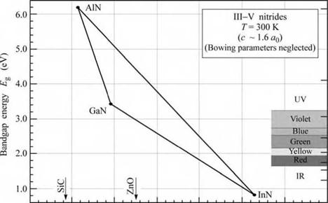
Fig. 12.12. Bandgap energy versus lattice constant of III—V nitride semiconductors at room temperature. 300 |
|
С << 400 «5 500 - З 600 $ 700 800 1000 |
|
3.0 3.1 3.2 3.3 3.4 3.5 3.6 3.7 Lattice constant a0 (A) |
The bandgap energy versus the lattice constant in the nitride material family is shown in Fig. 12.12. Inspection of the figure indicates that GaInN is, in theory, suitable for covering the entire visible spectrum. However, the growth of high-quality GaInN becomes increasingly more difficult as the In composition is increased, in part due to re-evaporation of In from the growth surface. As a result, the GaInN material system is exclusively used for ultraviolet (UV), blue, and green LEDs at the present time and rarely for longer wavelengths.
Prior to the year 2002, the generally accepted value for the InN bandgap energy was 1.9 eV. However, Wu et al. (2002a, 2002b) showed by luminescence measurements that the bandgap of InN is lower, namely between 0.7 and 0.8 eV. Luminescence measurements also indicated that the InN bandgap exhibits an unusual blue shift with increasing temperature.
|
|


 Опубликовано в