Effect of heterojunctions on device resistance
 9 марта, 2014
  admin
admin The employment of heterostructures allows one to improve the efficiency of LEDs by confining carriers to the active region, thereby avoiding diffusion of minority carriers over long distances. Heterostructures can also be used to confine light to waveguide regions; in particular, in edge - emitting LEDs. Generally, modern semiconductor LEDs and lasers have many heterojunctions, e. g. for contact layers, active regions, and waveguiding regions. Although heterostructures allow for improved LED designs, there are also problems associated with heterojunctions.
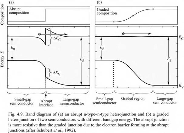
One of the problems introduced by heterostructures is the resistance caused by the heterointerface. The origin of the resistance is illustrated in Fig. 4.9 (a), which shows the band diagram of a heterostructure. The heterostructure consists of two semiconductors with different bandgap energy and it is assumed that both sides of the heterostructure are of n-type conductivity. Carriers in the large-bandgap material will diffuse over to the small-bandgap material where they occupy conduction band states of lower energy. As a result of the electron transfer, an electrostatic dipole forms, consisting of a positively charged depletion layer with ionized donors in the large-bandgap material, and a negatively charged electron accumulation layer in the small-bandgap material. The charge transfer leads to the band bending illustrated in Fig. 4.9 (a). Carriers transferring from one semiconductor to the other must overcome this barrier by either tunneling or by thermal emission over the barrier. The resistance caused by heterojunctions can have a strong deleterious effect on device performance, especially in high - power devices. The thermal power produced by heterostructure resistances leads to heating of the active region, thereby decreasing the radiative efficiency.
It has been shown that heterostructure band discontinuities can be completely eliminated by grading of the chemical composition of the semiconductor in the vicinity of the heterostructure (Schubert et al., 1992). The band diagram of a graded heterostructure is shown in Fig. 4.9 (b). Inspection of the figure reveals that there is no longer a spike in the conduction band which hinders the electron flow. It has been shown that the resistance of parabolically graded heterostructures is comparable to bulk material resistance. Thus, the additional resistance introduced by abrupt heterostructures can be completely eliminated by parabolic grading.
|
|
The shape of the graded region should be parabolic for the following reason. The large - bandgap material will be depleted of free carriers due to electron transfer to the small-bandgap material. Thus the charge concentration in the large-bandgap material will be the donor concentration. Assuming that the donor concentration ND is a constant throughout the heterostructure, the solution of the Poisson equation yields the electrostatic potential
(4.21)
|
|
The equation reveals that the potential depends quadratically on the spatial coordinate x, i. e. the potential has a parabolic shape. In order to compensate for the parabolic shape of the depletion potential, the composition of the semiconductor is varied parabolically as well, so that an overall flat potential results. It is assumed here that the parabolic variation of the chemical composition results in a parabolic change of the bandgap energy, i. e. that the bandgap energy depends linearly on the chemical composition and that bandgap bowing can be neglected.
|
|
Next, an approximate design rule for the grading of a heterostructure is given. Assume that the conduction band discontinuity of an abrupt heterojunction is given by AEC and that the structure is uniformly doped with doping concentration ND. Let us assume that carriers have transferred to the small-bandgap semiconductor, thus causing a depletion region of thickness WD in the large-bandgap semiconductor. If the potential created in the depletion region is equal to AEC / e, then electrons will no longer transfer to the small-bandgap material. The thickness of the depletion region can be inferred from Eq. (4.21) to be
(4.22)
A heterostructure interface should be graded over the distance WD in order to minimize the resistance introduced by an abrupt heterostructure. Although the result of Eq. (4.22) is an
approximation it provides excellent guidance for device design. Steps can be taken to refine the
calculation. For example, the potential change due to the electron accumulation layer in the small-bandgap material can be taken into account. Several software packages are available that allow for the numerical calculation of semiconductor heterostructures, for example the software package Atlas by the Silvaco Corporation.
Exercise: Grading of heterostructures. Assume that the conduction band discontinuity of an AlGaAs/GaAs heterostructure is given by AEC = 300 meV and that the structure is uniformly doped with donors of concentration ND = 5 x 1017 cm-3. Over what distance should the interface be graded in order to minimize the resistance occurring in abrupt heterostructures?
Solution: Calculating the depletion layer thickness from Eq. (4.22) yields WD = 30 nm. Thus the heterostructure should be graded over 30 nm to minimize the heterostructure resistance. The graded region should have two parabolic regions as shown in Fig. 4.9 (b).
Grading is useful for all heterostructures, including the heterostructures adjoining the active
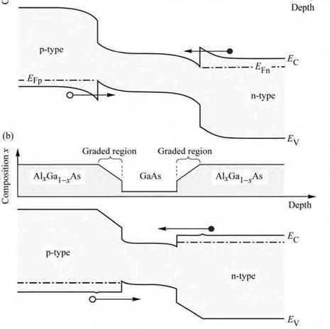
region. The effect of grading in a double heterostructure is shown in Fig. 4.10. The composition and the band diagram of an ungraded structure are shown in Fig. 4.10 (a). At both heterointerfaces, barriers develop as a result of free charge transferring to the active region. These barriers increase the device resistance under forward-bias conditions.
(a)
|
і Barrier region |
Active region |
Barrier region |
|
|
* "'I |
|||
|
AlxGaj^As |
GaAs |
AlvGa)xAs |
|
|
|
Fig. 4.10. Band diagram of (a) an abrupt double heterostructure and (b) a graded double heterostructure. The barrier—well interface of the abrupt junction is more resistive than the graded junction due to barriers forming at the interfaces. |
The case of graded heterointerfaces is shown in Fig. 4.10 (b). The figure shows two linearly graded regions cladding the active region. The band diagram illustrates that barriers at the heterointerfaces can be effectively reduced or completely eliminated by grading. Note that the linear grading shown in Fig. 4.10 (b) results in small “spikes” at the interfaces between the linearly graded and the non-graded regions. These “spikes” are a result of the linear grading assumed, and would not result for parabolic grading.
Generally, the transport of carriers in heterostructures should be as adiabatic as possible, i. e. the carrier transport within the semiconductor device should not generate unnecessary heat. This is particularly true for high-power devices where additional heat generated inside the device leads to a performance loss due to increased operating temperature.
Finally, note that lattice matching is desirable in all heterostructure devices. It is also desirable in graded structures in order to minimize the number of misfit dislocations that act as non-radiative recombination centers.


 Опубликовано в