Deviations from the ideal I-V characteristic
 6 марта, 2014
  admin
admin The Shockley equation gives the expected theoretical I-V characteristic of a p-n junction. To describe experimentally measured characteristics, the following equation is used:
I = IseV (nideal kT) (4.10)
where nideal is the ideality factor of the diode. For a perfect diode, the ideality factor has a value of unity (nideal = 1.0). For real diodes, the ideality factor assumes values of typically nideal = 1.11.5. However, values as high as nideal = 2.0 have been found for III-V arsenide and phosphide diodes. Values as high as nideal = 7.0 have been found for GaN/GaInN diodes. For a detailed analysis of the diode ideality factor see, for example, Rhoderick and Williams (1988), and Shah et al. (2003).
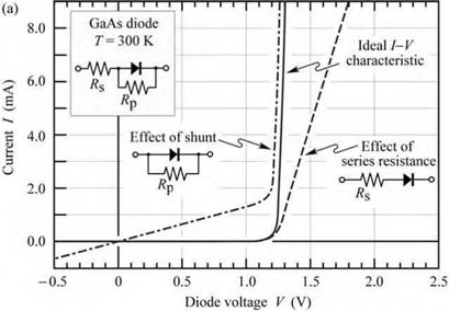
Frequently a diode has unwanted or parasitic resistances. The effect of a series resistance and a parallel resistance is shown in Fig. 4.4 (a). A series resistance can be caused by excessive contact resistance or by the resistance of the neutral regions. A parallel resistance can be caused by any channel that bypasses the p-n junction. This bypass can be caused by damaged regions of
the p-n junction or by surface imperfections.
|
|
The diode I-V characteristic, as given by the Shockley equation, needs to be modified in order to take into account parasitic resistances. Assuming a shunt with resistance Rp (parallel to the ideal diode) and a series resistance Rs (in series with the ideal diode and the shunt), the I-V characteristic of a forward-biased p-n junction diode is given by
(4.11)
|
Diode voltage V |
For Rp ^ да and Rs ^ 0, this equation reduces to the Shockley equation.
|
|
|
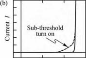
Fig. 4.4. (a) Effect of series and parallel resistance (shunt) on I-V characteristic, (b) I-V with clearly discernable subthreshold turn-on, caused by defects or surface states. |
Occasionally, the diode turn-on is distributed over a range of voltages rather than occurring abruptly at the threshold voltage. Both types of turn-on are shown in Fig. 4.4 (b). The non-abrupt turn-on is referred to as sub-threshold turn-on or premature turn-on. The sub-threshold current can be caused by carrier transport through surface states or deep levels in the bulk of the semiconductor.
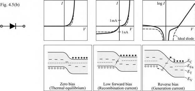
Detailed inspection of the diode I-V characteristic on a linear as well as logarithmic scale allows for the diagnosis of potential problems such as shunts, series resistances, premature turnon, and parasitic diodes. Figure 4.5 shows a number of parasitic effects that can occur in diodes. The diagrams may allow the reader to diagnose and identify specific problems in diodes.
4.2 Deviations from the ideal I-V characteristic Linear scale Negative current scale magnified Log scale
|
/ |
1 |
|
V |
|
1 mA-- z?:. |
|
1 nA |
|
log/ |
/ |
|
( V |
|
|
|
Ideal diode. The ideal diode I-V characteristic is given by the Shockley equation. |
Depletion region generation and recombination. The Shockley diode equation does not account for carrier generation and recombination events in the depletion region. However, in practical diodes, there are trap levels in the depletion region, which make such events likely. Carrier generation and recombination causes an excess current for both forward and reverse bias. In the forward-bias regime, the excess current is due to the recombination of minority carriers in the depletion region. This recombination current dominates only at low voltages and gives an ideality factor of 2.0. At higher voltages, the diffusion current dominates resulting in an ideality factor of 1.0. In the reverse-bias regime, the excess current is due to the generation of carriers in the depletion region. Under the influence of the electric field in the depletion region, generated carriers drift to the neutral regions. This generation current keeps increasing with reverse voltage due to the increasing depletion-layer width.
|
Photocurrent. In a practical measurement within a lighted room, a diode located in a transparent package generates a photocurrent. Therefore measurements need to be carried out |
in the dark. Switching off room lights or covering the setup with a dark cloth helps in reducing the photocurrent. In the dark, at zero voltage, there should be zero current. However, a very small non-zero current (e. g. 10-12 A) is frequently measured. The non-zero current is usually due to the limited accuracy of the measurement instrument. The best instruments will measure a current of about 10-15 A at zero bias, even if the measurement is carried out in total darkness (10-15 A = 1 atto ampere = 10-3 pA).
|
/ 1mA- |
J |
|
V - InA |
|
|
Fig. 4.5(d) |
|
|
|
/ |
m |
|
1 |
У |
|
1 |
|
|
Rs/ |
|
Rs o——о |
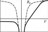
Diode with series resistance: A diode with a series resistance shows a deviation from the exponential behavior at high forward currents. According to Kirchhoff s voltage law, the voltages across the diode and the resistor add up. Note that a simple resistor has a linear and a logarithmic shape of the I-V characteristic when plotted on a linear and semi-logarithmic scale, respectively.
|
i |
i,/ |
|
V |
|
'P -O |
|
Fig. 4.5(e) *+ |
|
1mA- |
|
|
/ |
V -InA |
|
log / |
(7 Rp |
|
----------- |
V |
|
\ |
|
|
1 |
11 |
|
il |
11 |
Diode with parallel resistance (shunt): According to Kirchhoff s current law, the currents through diode and resistor add up. Note that the forward “hump” seen on the semi - logarithmic plot has about the same level as the reverse saturation current. This is a characteristic by which a shunt can be identified.
|
|
Diode with series and parallel resistance (shunt): Effects of shunt and series resistance found at low and high currents, respectively.
|
|
Parasitic diode with lower barrier height and smaller area than main diode. Such diodes display premature tum-on caused by leakage through either surface states at the perimeter of the diode chip or defective regions within the p-n junction plane that have a lower barrier height than the main p-n junction. Note that the forward “hump” on the semi-logarithmic plot has much higher level than the reverse saturation current, which is not the case for diodes with a shunt.
Exercise. Critical points of diode current-voltage characteristics. The I-V characteristics of diodes are frequently characterized in terms of four critical points, namely forward voltage one, Vf1, forward voltage two, Vf2, forward voltage three, Vo, and reverse saturation current, Is, specified at the operating current (e. g. 100 mA), a small forward current (e. g. 10 pA), a very small forward current (e. g. 1 pA), and at negative bias (e. g. - 5 V), respectively. The critical points are shown in Fig. 4.6.
(a) Explain the relevance of the critical points.
(b) Two GaInN diodes have the following data. (1) Vf1 = 3.2 V, VQ = 2.5 V, Vs = 2.3 V, Is = 0.8 pA; (2) Vf1 = 3.4 V, f = 2.0 V, Vf3 = 1.8 V, Is = 0.8 pA. Which device has the more favorable characteristics?
Solution. (a) For devices emitting at the same peak wavelength, Vf1 should be as low as possible, as high values indicate a high series resistance. The forward voltage two, Vf2, should be as high as possible (as close to Ffi as possible), as low values of VG indicate excessive sub-threshold leakage. The same argument applies to Vf3. The reverse saturation current should be as low as possible as high values of Is indicate excessive leakage paths (e. g. surface leakage or bulk leakage mediated by surface states, bulk point defects and dislocations). Low values of Vfl, high values of VG and Vf3, and low values of Is are consistently correlated with high device reliability. (b) Device (1) has more favorable characteristics due to lower series resistance and lower sub-threshold leakage.
|
---- 1--- Г" |
1--- Г I I |
|||
|
- |
100 mA^ |
|||
|
- |
I |
- |
||
|
- |
-5 V |
lOpA-, 1 pA-^_ |
1 - ( 1 |
|
|
- |
7s |
r-'V S ’ у Ff3 Vn *fl |
||
|
- |
і і i |
1 1 1 |
1 1 |
1 |
Fig. 4.6. Critical points of diode I-V characteristic, namely “forward voltage one”, Kj-| (measured at operating current, e. g. 100 mA), “forward voltage two”, Vf2 (measured at low current, e. g. 10 pA), “forward voltage three’ ’« Vfb (measured at very low current, e. g. 1 pA), and reverse saturation current (measured at e. g. - 5.0 V).
4.3 Evaluation of diode parasitic resistances The diode parallel resistance can be evaluated near the origin of the I-V diagram where V << Eg / e. For this voltage range, the p-n junction current can be neglected and the parallel
4 LED basics: electrical properties resistance is given by
Rp ~ dV/dl |nearorigin • (412)
Note that in any reasonable diode, the parallel resistance is much larger than the series resistance so that the series resistance need not be taken into account when evaluating the parallel resistance.
The series resistance can be evaluated at a high voltage where V> Eg / e. For sufficiently large voltages, the diode I-V characteristic becomes linear and the series resistance is given by the tangent to the I-V curve, as shown in Fig. 4.7 (a).
Rs = dV/dI I at voltages exceeding turn-on - (413)
However, it may not be practical to evaluate the diode resistance at high voltages due to device heating effects. For this case, the following procedure will be suitable.
|
~n~ |
|
.(a) |
|
с a •_ 3 U |
|
Slope = }/Rs і Vb JL I J I L Diode voltage V |
|
■ (b) |
1 1 1 |
|
|
/dK/d/ = RsI + kT/e |
- |
|
|
i i Ф % |
||
|
- |
<S ■ ■ |
- |
|
- ^ |
■ |
|
|
і і і |
|
-a |
|
Diode current / |
|
Fig. 4.7. Methods for evaluating diode series resistance, (a) Tangent for V > V[\ provides R$. (b) Equation shown as inset is valid for forward bias (V» kT/e). |
For devices with a high parallel resistance (Rp ^ да), the diode I-V characteristic, given in Eq. (4.11), can be written as
I = I e e (V-IRs)/(nideal kT) (4 14)
Solving the equation for V and then differentiating V with respect to I yields
dV = rs + nidealkT 1 (415)
dI e I
where the second summand on the right-hand side of the equation represents the differential p-n junction resistance. Multiplication of the equation by I allows one to identify the series resistance
of the diode as the slope of a (I dV / dI )-versus-I plot, as shown in Fig. 4.7 (b).


 Опубликовано в