Current crowding in LEDs on insulating substrates
 20 марта, 2014
  admin
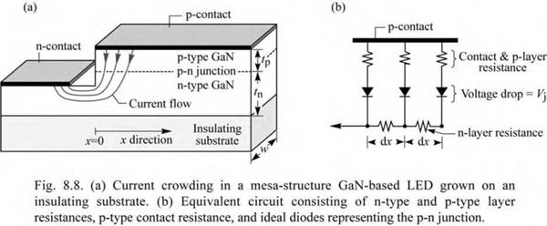
admin Current crowding also occurs in mesa-structure LEDs grown on insulating substrates. This type of LED includes GalnN/GaN LEDs grown on sapphire substrates. In these LEDs, the p-type contact is usually located on the top of the mesa, and the n-type contact is located on an n-type buffer layer at the bottom of the mesa. As a result, the current tends to crowd at the edge of the mesa contact adjoining the n-type contact.
|
(8.11) |
A lateral p-side-up mesa LED grown on an insulating substrate is shown in Fig. 8.8 (a). It is intuitively clear that the p-n junction current crowds near the edge of the mesa as indicated in the figure. An equivalent circuit model is shown in Fig. 8.8 (b) and includes the p-type contact resistance and the resistances of the n-type and p-type cladding layers. The p-n junction is approximated by an ideal diode. The circuit model also shows several nodes separated by a distance dx. Assuming that V is the voltage in the n-type layer along the x-direction, then dV is the voltage drop across the n-layer resistance of length dx. The incremental current flowing downward through one of the diodes is given by dI = Jo [exp (eVj / kT) - 1] w dx, where Jo is the saturation current density of the p-n junction. Calculating the difference in voltage drop between two adjacent resistors and applying Kirchhoff’s current law to the node located between the two resistors yields the differential equation
|
f eVj > |
||
|
exp |
- 1 |
|
|
T k |
|
d2V _ P„ , ■ ~TJ o dx tn |
|
|
In the case of zero or negligible resistance of the p-type layer, it is dV = dVj. In this case, Eq. (8.11) can be easily solved and an analytic solution was given by Thompson (1980) who calculated the spreading length in p-n junction diodes grown on conductive substrates. In Thompson’s study, the material resistivity of the top p-type cladding layer was considered, but the lower n-type cladding layer resistivity was neglected. However, in GaN/InGaN LEDs with the p-type layer on top and the n-type layer underneath, the resistive n-type layer causes current crowding and cannot be neglected. Furthermore, p-type resistances can be high, so that they should not be neglected either. As will be shown in the following calculation, both types of resistances play peculiar roles in the current-crowding problem.
Next, we take into account the resistance of the n-type layer, p-type layer, and the p-type contact resistance. The voltage drop across the p-n junction and the p-type resistors is given by
V = RvI0 [exp (eVj /kT)- 1 ] + Vj (8.12)
where Rv (“vertical resistance”) is the sum of the p-type layer resistance and the p-type contact resistance of the area element w dx, that is
tp 1
Rv = Pp wr + Pc (8ЛЗ)
w dx w dx
where pp is the resistivity of the p-type layer and pc is the p-type specific contact resistance. Forming the second derivative of V with respect to x in Eq. (8.12) and inserting the result into Eq. (8.11) yields the differential equation
|
2 |
|
d2Vj |
|
d2 V |
|
f eVj_} V kT ) |
|
Pn J —J0 n |
|
j _ |
|
.(8.14) |
|
1 |
|
+ |
|
exp |
|
dx2 |
|
v dx ) |
|
dx |
|
e ( )r feVj 1 kT (c + Pptp)J0exp |
|
V kT ) |
|
e f dVj 1 |
|
+ 2 kT |
In order to solve the differential equation, we restrict ourselves to the forward-bias operation of the diode. In this case, the junction voltage is much larger than kT/ e, that is
|
(8.15) |
Vj >> kT / e and exp (eVj / kT) >> 1 .
Furthermore, we assume that the voltage drop across the p-type series resistance and contact resistance is much larger than kT / e
|
(8.16) |
(Pc + Pptp) Joexp(eVj/kT) >> kT/e.
This condition applies to typical GaN/GaInN LEDs. Using the approximations of Eqs. (8.15) and (8.16), Eq. (8.14) can be simplified to
|
d2Vj |
|
f dV, >1 v dx ) |
|
kT |
|
Pn |
|
1 e ~~ + |
|
(8.17) |
|
(Pc + Pp tp) tn e |
|
kT |
|
dx2 |
Solving Eq. (8.17) for Vj yields Vj(x) = Vj(0) - (kT/e) (x /Ls). Inserting Vj into the equation J = J0 exp (eVj/kT) yields the solution of the differential equation as
|
(8.18) |
J(x) _ J(0) exp (- x / Ls)
where J(o) is the current density at the p-type mesa edge and Ls is denoted as the current spreading length, that is, as the length where the current density has dropped to the 1 / e value of the current density at the edge, so that J(Ls) / J(0) = 1/ e. The current-spreading length is given by
|
(8.19) |
Ls _ - J (Pc + Pptp) tn / Pn
Equation (8.19) shows that the current distribution depends on epitaxial layer thicknesses and material properties. A thick low-resistivity n-type buffer layer is needed to ensure that current crowding is minimized. Equation (8.19) also illustrates a somewhat surprising result; namely that the decrease of p-type specific contact resistance or p-type layer resistivity enhances the current-
crowding effect. For low p-type contact and confinement resistances, strong current crowding results, unless the n-type buffer layer is very conductive so that tn/p is very large. In GaN/GaInN devices, the sum of p-type contact and p-type layer resistances can be larger than the n-type cladding resistance, especially if tn is small.
|
|
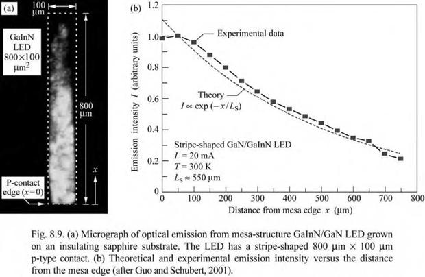
An experimental result on the current-crowding effect in GalnN/GaN LEDs grown on a sapphire substrate is shown in Fig. 8.9 (Guo and Schubert, 2001). A micrograph of the optical emission from a GaInN LED is shown in Fig. 8.9 (a). The picture was taken from the sapphire substrate side of the LED and shows the intensity of blue light emission. The micrograph clearly reveals that the emission intensity decreases with increasing distance from the mesa edge. Figure 8.9 (b) shows the experimental intensity as a function of the distance from the mesa edge. Also shown is a theoretical fit to the experimental data using the exponential decrease in current density derived above. The experimental and the theoretical data exhibit very good agreement if a current-spreading length of 550 |um is used in the calculation.
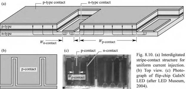
High contact resistances and high p-GaN resistivity are not desirable for high-power devices since these resistances generate heat. On the other hand, these resistances alleviate the current crowding effect. Note that with the expected future improvement of the contact and p-type doping in GaN devices, and larger device and contact sizes, current crowding will become increasingly severe unless novel contact geometries are introduced to alleviate the problem. Such novel contact geometries can include interdigitated structures (Guo et al., 2001; Steigerwald et al., 2001) with p-type finger widths of less than Ls. For device dimensions much smaller than Ls, the current-crowding effect becomes irrelevant.
|
|
The schematic structure and a photograph of an interdigitated stripe-contact geometry are shown in Fig. 8.10. Uniform current injection into the active region is achieved by the p-type contact width (Wp. contact) being smaller than the current spreading length. The width of the n-type contact (Wn-contact) must be at least equal to the contact transfer length to ensure low contact resistance. The contact transfer length follows from the transmission line model (TLM) used for characterization of ohmic contacts (see, for example, Schroder, 1998).
8.2 Lateral injection schemes A device structure with a lateral current-injection scheme is shown in Fig. 8.11 (a). The current is transported laterally in both the n-type and p-type cladding layers. Ideally, the light would be generated in the region between the contacts where they would not hinder the extraction of light. If the n-type sheet resistance pn / tn (where pn and tn are the resistivity and layer thickness of the n-type material, respectively) is much lower than the p-type sheet resistance pp / tp, the current prefers to flow laterally in the low-resistance n-layer rather than the p-layer. As a result, the junction current crowds near the p-type contact.
|
|
A schematic equivalent circuit suitable for the quantitative analysis is shown in Fig. 8.11 (b) where a p-n junction current density of J(0) is assumed at the edge of the p-type contact. The analytic solution of the equivalent circuit shown in Fig. 8.12 (Joyce and Wemple, 1970; Rattier et al., 2002) is an exponential given by
|
(8.20) |
J(x) = J(0) exp (- x/Ls)
where
|
(8.21) |
|
Ls |
2 Fa
J(0)[(pp/ tp) + (pn / tn)]
J(x = 0) = J(0) is the current density at the edge of the contact. Rattier et al. (2002) stated that the voltage Fa would be an activation voltage with magnitude of a few times kT/e, e. g. 50-75 mV.
|
|
For uniform light generation across the gap between the contacts, it is desirable to have a long exponential decay length Ls. This can be achieved by high doping or thick confinement layers. To attain high powers, one may be tempted to scale the device structure in size. However, for large contact separations L, the device becomes generally more resistive unless very thick confinement layers are being used (which may be unpractical). Scaling such device structures
can be accomplished by employing arrays of many small devices rather than scaling up a single device.
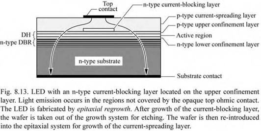
8.3 Current-blocking layers In conventional DH LEDs with small top contacts and large backside contacts, the current injected by the top contact enters the active region predominantly under the top contact. The extraction of light generated in the active region is thus strongly hindered by the opaque metal contact. One possibility to alleviate this problem is the use of a thick current-spreading layer. Another possibility is the use of a current-blocking layer. This layer blocks the current from entering the active region below the top contact. The current is deflected away from the top contact, thus allowing for higher extraction efficiency.
The schematic structure of an LED employing a current-blocking layer is shown in Fig. 8.13. The blocking layer is located on top of the upper confinement layer and has approximately the same size as the top metal contact. The current-blocking layer has n-type conductivity and is embedded in material with p-type conductivity. Owing to the p-n junction surrounding the current-blocking layer, the current flows around the current-blocking layer as indicated in Fig. 8.13.
|
|
Current-blocking layers can be fabricated by epitaxial regrowth. In this process, the DH and the thin n-type current-blocking layer are grown over the entire wafer surface. Subsequently, the wafer is taken out of the growth system for etching. The regions to be etched are defined by photolithography. The entire blocking layer is etched away except the region where the top ohmic contact is going to be located, as shown in Fig. 8.13. Frequently, the current-blocking - layer etch is selective so that it does not etch into the upper confinement layer. Subsequently, the wafer is returned to the growth system for resumption of epitaxial growth, i. e. for the growth of the current-spreading layer.
Regrowth processes are expensive due to the reduction of the device and wafer yield that usually accompanies regrowth processes. Cleaning of the wafer surface after the etching, directly before regrowth, is critical. Defects occurring at the regrowth interface can lead to a reduction in yield. Therefore, processes requiring epitaxial regrowth are more expensive and are not suited for low-cost devices. However, for more expensive devices, such as communication LEDs, epitaxial regrowth processes are used.
In AlGaInP LEDs, n-type GaAs has been used as the current-blocking layer. The n-type GaAs layer is located on top of the AlGaInP upper confinement layer. The GaAs current- blocking layer is lattice matched to the underlying AlGaInP confinement layer. Selective wet chemical etches are available that etch the GaAs but do not etch the AlGaInP (Adachi and Oe, 1983).
Vertical-cavity surface-emitting lasers (VCSELs) also employ current-blocking layers to funnel the current to the active region located between the mirrors of the laser. However, oxygen or hydrogen implantation rather than epitaxial regrowth is used in VCSELs to form current - blocking layers. The implantation depth is limited so that the lateral resistance can become substantial for devices with large-area contacts.


 Опубликовано в