Cross-shaped contacts and other contact geometries
 22 марта, 2014
  admin
admin Different requirements need to be satisfied by the top contact. In regular LEDs, the top contact provides a pad for the bonding wire. The pad is usually circular with a typical diameter of 100 ^m. The top contact pad also provides a low-resistance ohmic contact to the current - spreading layer.
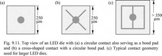
Typical top contact geometries are shown in Fig. 9.11. The simplest geometry is just a circular contact pad, as shown in Fig. 9.11 (a). A cross-shaped contact, as shown in Fig. 9.11 (b), provides a more uniform current distribution over the entire area of the active region. Note, however, that no or little current should flow to the edges of the LED die to avoid surface recombination.
|
|
For large-area LEDs, a simple circular pad or a cross-shaped top contact are insufficient for uniform current distribution. In such large-area devices, patterns that include a ring, as shown in Fig. 9.11 (c), are better suited to providing uniform current distribution.
The area of the top contact is kept small so that the light emanating from the active region is not hindered by the opaque contact. However, the contact resistance scales with the contact area so that the top contact area cannot be scaled down arbitrarily.


 Опубликовано в