Transparent substrate technology
 22 марта, 2014
  admin
admin Visible-spectrum (AlxGa1-x)05In05P LEDs with typical operating wavelengths of 560-660 nm are grown lattice matched on GaAs substrates. Since the energy gap of GaAs is Eg = 1.424 eV
(Xg = 870 nm) at room temperature, GaAs substrates are absorbing at these emission wavelengths. As a result, the light emitted towards the substrate will be absorbed by the thick GaAs substrate. Thus, the extraction efficiency of AlGalnP/GaAs LEDs grown on GaAs substrates is low.
|
OMVPE AlGaInP epi growth |
|
Absorbing GaAs substrate |
The extraction efficiency of AlGaInP LEDs can be increased substantially by removal of the GaAs substrate and bonding of the epitaxial layer to a GaP substrate (Kish et al., 1994). GaP is an indirect-gap semiconductor with Eg = 2.24 eV (Xg = 553 nm). Thus, GaP does not absorb light with X > 553 nm emitted by the AlGaInP active region.
|
" 7Г ■ GaP window |
К/ GaP window |
|||||
|
GaP window |
GaP window |
|||||
|
///////// |
///////// |
|||||
|
Absorbing |
Absorbing |
4 |
Transparent |
4 |
Transparent |
|
|
GaAs substrate |
GaAs substrate |
GaP substrate |
GaP substrate |
|
і—AlGaInP DH [ZZZZZZZZZ |
|
VPE GaP window growth |
|
GaAs substrate removal GaP wafer bonding with with uniaxial pressure wet chemical etch at elavated temperatures |
|
AIGalnP/GaP TS w'afer |
|
Fig. 9.12. Schematic fabrication process for wafer-bonded transparent substrate (TS) AIGalnP/GaP LEDs. After the selective removal of the original GaAs substrate, elevated temperature and uniaxial pressure are applied, resulting in the formation of a single TS LED wafer (after Kish et al., 1994). |
The fabrication process of the AlGaInP LEDs wafer-bonded to a GaP substrate is illustrated schematically in Fig. 9.12. The AlGaInP double heterostructure (DH) is initially grown by OMVPE on a GaAs substrate. Subsequently, a thick GaP window layer (~ 50 ^m) is grown on the DH by chloride VPE, a growth technique that allows for the low-cost growth of thick epitaxial layers. The GaAs substrate is then removed using a wet chemical selective etching process (Adachi and Oe, 1983; Kish et al., 1994). During the removal of the GaAs substrate, the thick GaP window layer serves as a temporary mechanical support for the DH. The DH with the GaP window is then wafer-bonded to a GaP substrate.
|
Fig. 9.13. Current-voltage characteristic, forward voltage, and series resistance of absorbing-substrate (GaAs) and transparent-substrate (GaP) LEDs with AlGaInP active regions. |
|
....................................... AlGaInP LEDs |
I 1 kS TS |
|||
|
X = 590 nm T = 300 к |
/ |
|||
|
Absorbing substrate (AS): - Vf at 20 mA = 1.95 V /?s = 4 £2 |
||||
|
Transparent substrate (TS): - Vf at 20 mA = 2.18 V Rs = 12 £2 |
||||
|
і l. I > |
1 |
------ |
|
0.0 0.5 1.0 1.5 2.0 2.5 Diode voltage V (V) |
|
The forward voltage is a critical figure of merit for wafer-bonded p-n junction devices. A low voltage indicates true semiconductor-to-semiconductor chemical bonding and an absence of interfacial oxide layers. The forward current-voltage characteristic of commercial absorbing - substrate (AS) and transparent-substrate (TS) AlGaInP LEDs is shown in Fig. 9.13. Inspection of the figure reveals that TS LEDs have a higher forward voltage and series resistance compared with AS devices. The higher forward voltage in TS devices is probably due to either ohmic losses occurring at the wafer-bonded interface or in the GaP substrate. A detailed analysis by O’Shea et al. (2001) confirmed that a forward-voltage penalty results from the wafer-bonded interface, particularly if this interface is either contaminated with carbon or crystallographically misaligned. The n-type |
Wafer-bonding processes require a high degree of cleanliness, the lack of any particles between the wafers, and the absence of native surface oxides on both wafers. Frequently, the gap between two wafers is filled with a contact liquid. Rotating the wafers at a high rate spins out the contact liquid. Kish et al. (1995) and Hoefler et al. (1996) reported an AlGaInP-to-GaP wafer-
bonding process, suitable for 50 mm (2 inch) GaP substrates. Uniaxial pressure and elevated temperatures (750-1000 °C) are used in this process (Hoefler et al., 1996). Kish et al. (1995) showed that the achievement of low-resistance ohmic conduction across wafer-bonded interfaces is critically dependent upon the crystallographic alignment of the bonded wafer surfaces, irrespective of the lattice mismatch between the surfaces. Furthermore, Kish et al. (1995) showed that the crystallographic surface orientation of the bonded surfaces must be nominally matched while simultaneously maintaining rotational alignment of the wafers. Low diode forward voltages of 2.2 V for AlGaInP/GaP LEDs are routinely achieved under high-volume manufacturing conditions with the process. The reliability of wafer-bonded LEDs is comparable to monolithic AlGaInP/GaAs LEDs. Usually the technical details of wafer-bonding processes are proprietary and not known to the general public.
doping concentration in the GaP substrate is kept moderately low, to minimize free-carrier absorption.
|
|
|
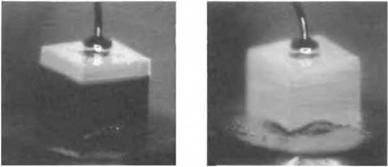
Figure 9.14 compares AlGaInP/GaAs AS LEDs with AlGaInP/GaP TS LEDs emitting in the amber wavelength range (Kish and Fletcher, 1997). The substrate appears dark for the AS LED, in contrast to the TS LED. Transparent substrate AlGaInP/GaP LEDs have a factor of 1.5-3.0 higher external efficiency compared with AS AlGaInP/GaAs LEDs. |
|
(a) AS LED (b) TS LED |
|
Fig. 9.14. (a) Amber AlGaInP |


 Опубликовано в