Current-spreading layer
 19 марта, 2014
  admin
admin In LEDs with thin top confinement layers, the current is injected into the active region mostly under the top electrode. Thus, light is generated under an opaque metal electrode. This results in a low extraction efficiency. This problem can be avoided with a current-spreading layer that spreads the current under the top electrode to regions not covered by the opaque top electrode.
The current-spreading layer is synonymous with the window layer. The term window layer is occasionally used to emphasize the transparent character of this layer and its ability to enhance the extraction efficiency.
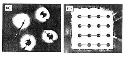
The usefulness of current-spreading layers was realized during the infancy of LEDs. Nuese et al. (1969) demonstrated a substantial improvement of the optical output power in GaAsP LEDs by employing a current-spreading or window layer. The window layer is the top semiconductor layer located between the upper cladding layer and the top ohmic contact. The effect of a current-spreading layer is illustrated in Fig. 8.1. Light is emitted only around the perimeter of the top contact for LEDs without a current-spreading layer, as shown in Fig. 8.1 (a). The addition of a current-spreading layer results in more uniform and brighter surface emission as shown in Fig. 8.1 (b).
Nuese et al. (1969) demonstrated current-spreading layers composed of the ternary GaAsP and the binary GaP and discussed the requirements of the current-spreading layer. These
requirements include low resistivity and large thickness for current spreading, and transparency to minimize absorption losses. To reduce absorption losses, Nuese et al. (1969) employed a high P mole fraction in the GaAs1-xPx current-spreading layer, namely 0.45 < x < 1.0, higher than the P mole fraction in the GaAs1-xPx active region, where x = 0.45. Thus the bandgap energy of the current-spreading layer is higher than the bandgap of the active region. Although Nuese et al. discussed the properties of the current-spreading layer qualitatively, they did not provide a quantitative theoretical framework of current spreading. The theoretical foundation of current - spreading layers in devices with linear contact geometry was given by Thompson, as discussed below. The use of a current-spreading layer was adopted in most top-emitting LED designs, including AlGaAs LEDs (Nishizawa et al., 1983; Moyer 1988), GaP LEDs (Groves et al., 1977, 1978a, 1978b), and AlGaInP LEDs (Kuo et al, 1990; Sugawara et al, 1991, 1992a, 1992b).
|
|
Fig. 8.1. Effect of the current-spreading layer on LED output, (a) Top view without a current-spreading layer. Emission occurs only near the perimeter of the contact, (b) Top view with a current - spreading layer (after Nuese etal., 1969).
The effect of the current-spreading layer is illustrated schematically in Fig. 8.2. Without a current-spreading layer, the current-injected area of the active region is limited to approximately the contact size, as indicated in Fig. 8.2 (a). The addition of the current-spreading layer results in a larger current-injected area, as shown in Fig. 8.2 (b).
Current-spreading layers are predominantly employed in top-emitting LEDs. Two different approaches for AlGaInP visible LEDs, grown on GaAs substrates, are shown in Figs. 8.2 (c) and (d). A GaP current-spreading layer was reported by Kuo et al. (1990) and Fletcher et al., (1991a, 1991b). GaP has a bandgap of £g, GaP = 2.26 eV and is thus transparent for red, orange, yellow, and part of the green spectrum. AlGaInP LEDs with emission wavelengths as short as 550 nm have been fabricated. GaP, as a binary compound semiconductor, is very transparent for energies below the bandgap, i. e. the Urbach tail energy of GaP is small. Furthermore GaP is an indirect-gap semiconductor, which is inherently less absorbing compared with direct-gap semiconductors. Thus little light is absorbed even in thick GaP current-spreading layers.
|
.Ohmic contact |
|
i- |
|
(с) |
— P-contact |
|
|
2-15 дт |
GaP window layer |
Mg-doped |
|
0.5 - 1 дт |
AllnP |
Mg-doped |
|
0.5 - 1 дт |
AlGaInP active |
undoped |
|
1.0 дт |
AllnP |
Te-doped |
|
n-type GaAs substrate |
Te-dopcd |
|
N-contact |
|
V Current spreading layer |
|
|
/ /__________ |
......... 4 |
|
<■"'/ / emission retnon ~.s |
|
|
/ — — — — — — — — |
------------- |
|
f f ' |
Substrate |
|
(b) |
|
Top confine ment I |
|
Active |
|
1 Bottom confine ment |
|
AlGaAs |
p-doped |
|
AlGaInP |
p-doped |
|
AlGaInP active |
undoped |
|
AlGaInP |
n-doped |
|
n-type GaAs substrate |
|
(d) |
|
P-contact |
|
• p~-GaAs |
|
N-contact |
Fig. 8.2. Current-spreading structures in high-brightness AlGaInP LEDs. Illustration of the effect of a current-spreading layer for LEDs (a) without and (b) with a spreading layer on the light extraction efficiency, (c) GaP current-spreading structure (Fletcher et al., 1991a, 1991b). (d) AlGaAs currect-spreading structure (Sugawara et al., 1992a, 1992b).
However, GaP is lattice mismatched to the underlying epitaxial layers. The lower confinement, active, and upper confinement layers are lattice matched to the GaAs substrate. Since GaP has a lattice constant that is about 3.6% smaller than that of GaAs, a high density of threading dislocations and stacking faults is expected at the upper-cladding-layer-to-GaP interface. One could assume that these dislocations, which will act as non-radiative recombination centers, will not degrade the internal quantum efficiency of the LED because they are located at the confinement-window layer interface and in the window layer, far away from the active region. However, if the dislocations propagated downward towards the active region during device operation, the efficiency and the reliability of the LEDs would be affected. The issues associated with the confinement-window interface have apparently been resolved since AlGaInP/GaAs LEDs with GaP window layers have excellent reliability and efficiency.
An alternative approach for increasing the extraction efficiency in AlGaInP/GaAs LEDs uses AlGaAs current-spreading layers (Sugawara et al., 1991, 1992a, 1992b). AlxGa1-xAs is lattice - matched to GaAs for all chemical compositions 0 < x < 1. Al As has a bandgap energy of -Eg, AiAs = 2.9 eV. For x > 0.45, AlxGa1-xAs becomes an indirect semiconductor. The absorption
coefficient of indirect semiconductors is much smaller than that of direct-gap semiconductors. The AlGaAs current-spreading layer is lattice matched to the underlying confinement layer and thus misfit dislocations, as in the case of GaP spreading layers, do not arise for AlGaAs current - spreading layers. However, the absorption of light in the AlGaAs layers is higher than the absorption in the GaP spreading layers. The AlGaAs is a ternary alloy and fluctuations of the cation concentration (Al and Ga) lead to a local variation of the bandgap energy. The compositional fluctuations lead to an absorption tail for energies below the AlGaAs bandgap so that AlGaAs has a larger Urbach energy than GaP.
|
Position across LED chip (mil.) |
It is well known that Al-containing compounds are difficult to grow by organo-metallic vapor-phase epitaxy (OMVPE), the common epitaxial crystal growth technique for LEDs. Aluminum is a very reactive element and OMVPE cleanliness is essential. Even minor leaks in the growth system will result in the degradation of Al-containing films. This applies, in particular, to compounds containing a high percentage of Al such as AlAs. The optical properties of AlGaAs current-spreading layers are therefore usually inferior to the properties of GaP spreading layers. The electrical properties of AlAs or AlGaAs with high Al content are also inferior to GaP. Finally, AlAs tends to oxidize over time when exposed to water or humid air (Choquette et al., 1997). Despite these difficulties, viable AlGaInP LEDs with AlGaAs current - spreading layers have been developed and are commercially available.
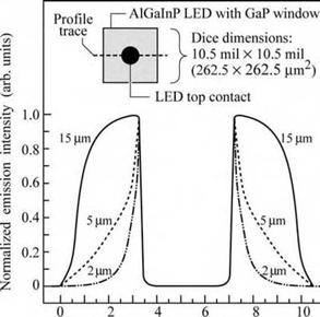
Fig. 8.3. The effect of GaP window thickness on current spreading is illustrated by surface light emission intensity profiles for three different Al - GalnP LED chips with window layer thicknesses of 2, 5, and 15 (im. The profile is indicated by the dashed line in the inset. The dip in the middle of the profiles is due to the opaque ohmic contact pad. A microscope fitted with a video camara was used in the measurements (after Fletcher et al., 1991 a).
The increase in light extraction efficiency is illustrated in Fig. 8.3 for p-type GaP current- spreading layer with a resistivity of 0.05 Q cm and thicknesses ranging from 2 to 15 |um
(Fletcher et al., 1991a). The data shown in Fig. 8.3 were obtained using a near-field microscope and a video analyzer. To obtain the light intensity profile, a single-line scan was taken across the chip, including the center p-type contact pad, as shown in the inset. Since the intensity is directly proportional to the p-n current density at any given point, the current-spreading characteristics are obtained by this measurement. For a window thickness of 2 |um, current spreading is limited. As the window layer thickness is increased to 15 |um, the current spreads well beyond the contact, reaching almost the edge of the chip. An even larger thickness of the window layer would spread the current to the edges of the chip. Such strong current spreading is not desirable due to surface recombination.
|
Forward current / (mA) |
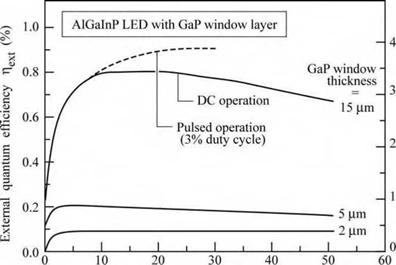
The effect of current spreading on the efficiency of an AlGaInP/GaAs LED with a GaP current-spreading layer is shown in Fig. 8.4. For as sufficiently thick window layer the extraction efficiency is increased by a factor of approximately 8. The comparison of pulsed with direct current (DC) measurements shown in Fig. 8.4 shows that the efficiency drop occurring at high currents is caused by heating of the device.
Fig. 8.4. Bare chip external quantum efficiency and luminous efficiency versus forward current for AlGaInP LEDs with GaP window layer thicknesses of 2, 5, and 15 (im. Solid curves are under DC conditions. Dashed curve is under pulsed condition using 400 ns pulses and a 3% duty cycle. Heating is essentially eliminated in this case (after Fletcher et a!., 1991a).
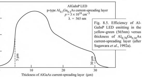
The optimum thickness range of current-spreading layers in AlGaInP/GaAs LEDs with Al070Ga030As current-spreading layers was investigated by Sugawara et al. (1991, 1992a, 1992b). The p-type doping concentration of the Al070Ga0 30As spreading layer was 3 x 1018 cm-3. The luminous efficiency of the LED versus current-spreading layer thickness is shown in Fig. 8.5. Inspection of the figure reveals that the optimum thickness of the current-spreading layer is between 5 and 30 |um. For a current-spreading layer thickness of 15 |um, the efficiency of
the device increases by a factor of 30 compared with a device with no current-spreading layer at all. The optimum doping concentration in the p-type current-spreading layer was found in the low 1018 cm-3 range.
|
|
0.8
0.6 ■
О
.2і и
E 0>
* 0.4 ■
з о с
Є з - J
0.2 •
0 :
0
The disadvantage of no or a very thin current-spreading layer is that most of the light is generated under the opaque metal contact pad, thereby hindering the escape of light from the LED die. A very thick window layer is equally disadvantageous. Firstly, a thick window layer spreads the current all the way to the edge of the LED dies, which leads to increased surface recombination and thus lowers the efficiency of the LED. Secondly, light absorption increases with the thickness of the window layer due to the absorption of below-bandgap light in the window layer. Thirdly, a thick window layer will increase the ohmic resistance of the device thereby lowering the overall efficiency. Fourthly, the long growth times required for thick current-spreading layers may result in the diffusion of dopants from the confinement layers into the active region, thereby lowering the internal quantum efficiency.
Current spreading is an important issue in many LED materials, in particular in those materials that possess low conductivity. Current spreading in the top p-type layer of GaN/GaInN LEDs is very weak due to the high resistivity of the p-type top cladding layer. The hole mobility in III-V nitrides is typically 1-20 cm2 / (V s) and the hole concentrations are in the 1017 cm-3 range, resulting in resistivities > 1 Q cm. To address this problem, Jeon et al. (2001) demonstrated an LED with a tunnel junction adjoining the p-type confinement region above the active region. An n-type layer on top of the tunnel junction allows for lateral current spreading
under the top contact. Owing to the employment of the tunnel junction, the LED has two n-type but no p-type ohmic contacts.
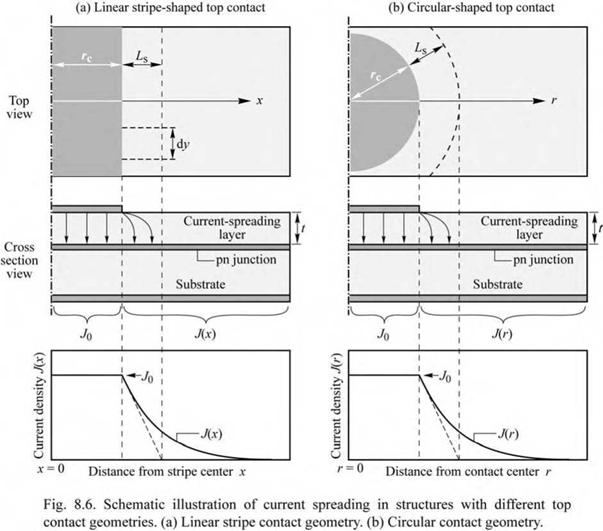
8.1 Theory of current spreading The theory of current spreading under a linear stripe top contact geometry has been reported by Thompson (1980). Such a stripe-like geometry is typical for semiconductor lasers. Figure 8.6 (a) shows the schematic cross section of a stripe-geometry semiconductor laser. The laser has a current-spreading layer located above the p-n junction. Because of the symmetry of the laser, only the right half of the laser is shown, so that the left edge of the contact shown in the diagram is actually the center of the laser stripe. The model assumes a constant potential and current density (J0) under the metal (x < rc). The potential throughout the substrate is assumed to be constant. The current density J(x) extending away from the contact is given by
|
J (x) |
|
(x > rc) |
|
(8.1) |
|
[x rc)/Ls + V2"" |
|
2 J0 |
where Ls is the current spreading length given by
|
(8.2) |
|
Ls _ |
t nidealkT
P J0 e
where p is the resistivity of the current spreading-layer, t is the thickness of the current-spreading layer, and nideal is the diode ideality factor. The diode ideality factor has typical values of
1.5 < nideal < 1.35.
We next develop a theoretical model that can be applied to linear stripe (see Fig. 8.6 (a)) as well as circular contact (see Fig. 8.6 (b)) shapes. We first consider the linear stripe contact geometry. We assume that the current at the edge of the spreading region (x = rc + Ls) is a factor of e-1 lower than under the metal contact. Then the voltage drop across the junction at the edge of the current-spreading layer is nideal kT / e lower than under the metal contact. This voltage drops within the current-spreading region. The resistance of the current-spreading region along the lateral direction per unit stripe length dy is given by
|
Ls |
|
R |
|
P |
|
t dy |
|
(8.3) |
|
|
The current flowing vertically through the junction in the current spreading region is given by
I = J0 Ls dy. (8.4)
Using Ohm’s law, one obtains
|
L |
|
(8.5) |
|
e |
|
P—J0 Lsdy = t dy |
|
= nidealkT |
Solving this equation for t yields
|
(8.6) |
t 2 T e t = p Ls J0
nidealkT
Comparison of this equation with Eq. (8.2) yields that the two equations are identical.
|
Equation (8.6) allows one to calculate the required current-spreading layer thickness t for a given resistivity of this layer and the desired current-spreading length Ls. We next consider the circular contact geometry shown in Fig. 8.6 (b). The circular geometry is relevant to LEDs with a circular top contact. Proceeding in a similar way, we write the lateral resistance from the edge of the contact to the edge of the current-spreading region. This resistance is given by |
|
Ls |
|
R = +Ls p_Ldr j rc A |
|
1 |
|
rc + Ls |
|
P |
|
I |
|
(8.7) |
|
dr |
|
ln |
|
1 + |
|
P |
|
12n r |
|
2nt |
|
r |
|
c |
|
'c У |
|
The current flowing vertically through the junction in the current spreading region is given by |
|
n (Ls + rc) |
|
= J0 n Ls (Ls + 2 rc) |
|
(8.8) |
|
I = J0 |
|
Using Ohm’s law, one obtains |
|
f L ^ 1 + —^ V rc У |
|
J0 n Ls ( + 2 rc) = "ideal kT |
|
P |
|
ln |
|
(8.9) |
|
2n t |
|
Solving this equation for t yields |
|
f L ^ 1 + Ls |
|
Ls |
|
e |
|
t = PLs I rc + |
|
ln |
|
J0 |
|
(8.10) |
|
nideal kT |
|
2 |
|
rc |
|
c У |
|
Equation (8.10) allows one to calculate the required current-spreading layer thickness t for a given resistivity of this layer and the desired current-spreading length Ls. Note that for large values of rc, we can simplify Eq. (8.10) using the approximation ln (1 + x) = x, valid for x << 1. Thus, in the limit of large values of rc (e. g. rc ^ ^), Eq. (8.10) and Eq. (8.6) become identical, as expected. |
|
Exercise: Current crowding occurring at very high current levels in devices with current-spreading layer. In device structures with vertical current flow (current flowing from top to bottom of chip), the current-spreading layer ensures that the current spreads out over the entire p-n junction area. However, as the current increases to very high levels, the current tends to crowd under the top contact. This is illustrated in Fig. 8.7 (a) and (b). Explain the phenomenon of current crowding occurring at very high current densities. Solution 1: The equation for the current-spreading length has the dependence Ls ^ J0-1/2. Thus, as the current density increases, Ls decreases, and the current “bunches” under the top contact. |
Solution 2: An intuitive explanation for current crowding can be obtained from the equivalent circuit shown in Fig. 8.7 (c). At very high current densities, the resistors that represent the p-n junction decrease (whereas the resistors representing the current-spreading layer remain constant), thereby causing the current to flow directly downward from the top contact.
|
(a) Low current (b) High current (c) Equivalent circuit
Fig. 8.7. Schematic current flow in device with current-spreading layer at (a) low and (b) high current. Current spreading decreases at very high current densities which results in current “bunching” under the top contact as shown in (b). (c) Equivalent circuit. |


 Опубликовано в