UV devices emitting at wavelengths longer than 360 nm
 2 апреля, 2014
  admin
admin UV devices emitting at wavelengths longer than 360 nm generally have GaN or GaInN active regions. GaInN LEDs with peak wavelengths ranging from 400 nm to 410 nm were reported as early as 1993 (Nakamura et al., 1993a, b, 1994). The design of an early GaInN UV LED emitting at 370 nm is shown in Fig. 13.13. The device has a GaInN/AlGaN double heterostructure active region and AlGaN electron - and hole-blocking layers (Mukai et al., 1998). The active region and the carrier-blocking layers are clad by p-type and n-type GaN.
|
-n-electrode |
p-electrode p-type GaN, 120 nm p-type Alo.15Gao.85N, 60 nm undoped GalnN, 40 nm n-type Alo.1Gao.9N, 30 nm n-type GaN, 4.0 pm GaN nucleation layer
Fig. 13.13. Layer structure of GalnN UV LED grown on sapphire substrate emitting at 370 nm (after Mukai et al.,
1998).
Sapphire substrate
|
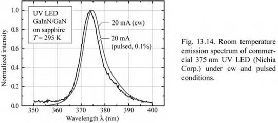
Figure 13.14 shows the emission spectrum of a 375 nm UV LED under pulsed and continuous wave (cw) injection conditions. Inspection of the figure reveals a small red-shift of the peak wavelength when going from pulsed to cw current injection. This shift is likely caused by junction heating, which generally leads to a lower bandgap energy and a red-shift of the emission wavelength.
|
|
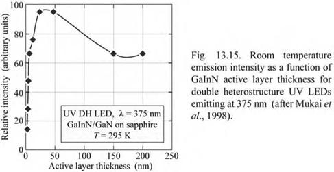
Figure 13.15 shows the emission intensity of a 375 nm UV LED as a function of the active layer thickness. The figure reveals that optimum output power is attained at 30-50 nm active layer thickness. It can be assumed that the active region is heavily doped in order to screen the polarization fields. Quantum well active regions with quantum well thicknesses < 5 nm reduce the effect of spatial electron-hole separation and for this reason, quantum well active regions have superseded the double heterostructure designs.
|
|
|
|
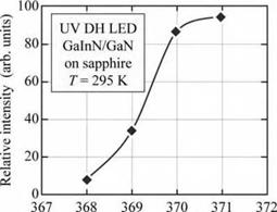
Figure 13.16 shows the dependence of the output power as a function of wavelength. As the emission wavelength decreases, a pronounced drop in the emission intensity is found. This has been attributed to the very positive influence of indium (In) incorporation on the internal quantum efficiency. The positive influence is reduced as less indium is incorporated in the active region with pure GaN active regions (k « 360 nm) not benefiting at all. |
|
Emission wavelength X (nm) |
|
Fig. 13.16. Room temperature intensity as a function of emission wavelength for GaInN double heterostructure UV LEDs (after Mukai et al., 1998). |
|
250 300 350 400 450 500 550 § 250 300 350 400 450 500 550 Wavelength X (nm) Wavelength X (nm) Fig. 13.17. Emission spectrum of deep-UV AlGaN/AlGaN multiple-quantum well LED for different injection currents on (a) linear and (b) logarithmic scales. An interdigitated contact geometry, as shown in (c), was used for large-area dies (after Fischer et a!., 2004). |


 Опубликовано в