Protection against electrostatic discharge (ESD)
 27 марта, 2014
  admin
admin Electrostatic discharge (ESD) can be a major failure mechanism for electronic and optoelectronic components (Voldman, 2004). Consider that a charge +Q is brought into contact with one of the diode electrodes. Consider further that the charge +Q is discharged uniformly over a time At, so
that a current of I = +Q / At flows through the device.
Let us first assume that the charge is brought into contact with the cathode of the LED and that the anode is grounded. The current will discharge with the diode in the reverse polarity. Taking the equivalent circuit of the reverse-biased diode as a capacitor C and a parallel resistor Rp, the voltage across the p-n junction in the steady state will rise to IRp. Thus the energy dissipated in the device during the reverse discharge is then given by I 2Rp At.
Let us next assume that the charge is brought into contact with the anode of an LED and that the cathode is grounded. The current will discharge with the diode in the forward polarity. Taking the equivalent circuit of the forward-biased diode as a voltage source with voltage Vth with a series resistor Rs, the steady-state voltage across the p-n junction is Vth + IRs, which, in the limit of a high current, can be approximated by IRs. Thus the energy dissipated in the device during the forward discharge is approximately I 2Rs At.
Because I 2Rp At >> I 2Rs At, it is evident that the energy dissipated per reverse discharge event is much higher than the energy dissipated per forward discharge event, suggesting that reverse discharges are more damaging than forward discharges. This contention has indeed been confirmed by experiments (Wen et al., 2004).
|
|
Wide-bandgap diodes (such as GaN-based diodes) are particularly prone to ESD failures, due to inherently high values of Rp (low reverse saturation currents and high breakdown voltages). This has spurred the development of ESD protection circuits for III-V nitride diodes (Steigerwald et al., 2002; Sheu, 2003).
|
|
|
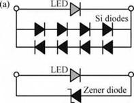
Fig. 11.5. (a) Electrostatic discharge (ESD) protection circuits using multiple Si p-n junctions, one Zener diode, and two Zener diodes, (b) ESD protection integrated into a Si submount (two-Zender diode circuit after Lumileds, 2004). |
Electrostatic discharge-protection circuits can consist of a series of Si diodes, one Si Zener diode, or two Si Zener diodes, as shown in Fig. 11.5, with two Zener diodes being a common configuration (Steigerwald et al., 2002; Lumileds, 2004). The current caused by an electrostatic discharge will bypass the LED and flow through the ESD protection circuit, particularly for reverse discharges. ESD protection circuits have been integrated with Si submounts (Steigerwald
et al., 2002; Lumileds, 2004). Using one or two Zener diodes or placing several Si diodes in series increases the threshold voltage of the ESD circuit to values beyond the turn-on voltage of the LED. Thus, under normal operating conditions, the current through the ESD circuit is negligibly small.
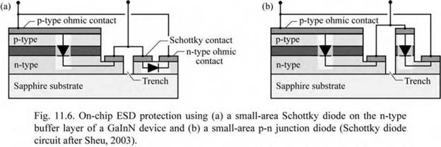
Sheu (2003) proposed a Schottky diode integrated with the LED on the same chip. The structure, shown in Fig. 11.6 (a), consists of a large-area p-n junction diode and, separated by a deep trench, a small-area Schottky diode. The Schottky diode, fabricated on the n-type buffer layer of a GaInN LED, is forward biased when the LED is biased in the reverse polarity. For reverse electrostatic discharges, the current flows mostly through the Schottky diode, thereby bypassing the p-n junction and preventing damage to the p-n junction. For forward electrostatic discharges, the current flows through the p-n junction. In an alternative structure, shown in Fig. 11.6 (b), the Schottky diode is replaced by a p-n junction diode (Cho, 2005).
|
|
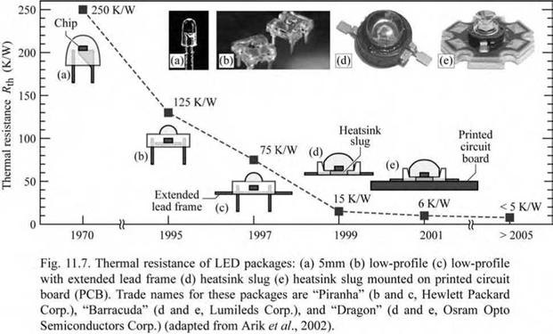
11.2 Thermal resistance of packages The thermal resistance of LED packages together with the maximum temperature of operation determines the maximum thermal power that can be dissipated in the package. The maximum temperature of operation may be determined by reliability considerations, by the degradation of the encapsulant, and by internal-quantum-efficiency considerations. Several types of LED packages and their thermal resistance are shown in Fig. 11.7 (Arik et al., 2002). Early LED packages, introduced in the late 1960s and still used for low-power packages at the present time, have a high thermal resistance of about 250 K/W. Packages using heatsink slugs made of Al or Cu that transfer heat from the chip directly to a printed circuit board (PCB), which in turn spreads the heat, have thermal resistances of 6-12 K/W. It is expected that thermal resistances of < 5 K/W will be achieved for advanced passively cooled power packages.
Note that the packages shown in Fig. 11.7 do not use active cooling, i. e. fan cooling. Heatsinks with cooling fins and fan are commonly used to cool electronic microchips including Si CMOS microprocessors. They have thermal resistances < 0.5 K/W. The use of active cooling devices would reduce the power efficiency of LED-based lighting systems.
|
|


 Опубликовано в