Dislocations in III-V nitrides
 2 апреля, 2014
  admin
admin The most common substrate for GaN epitaxial growth, sapphire, is a very stable substrate in terms of its thermal, chemical, and mechanical properties. However, sapphire has the complex corundum structure whereas III-V nitrides crystallize in the wurtzite structure. Furthermore, the lattice constants of sapphire and GaN are different. As a result, GaN epitaxial films have misfit dislocations (threading and edge dislocations) that are typically on the order of 108-
109 cm-2.
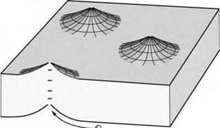
The initial stages of GaN growth on sapphire are shown schematically in Fig. 13.7 (Nakamura and Fasol, 1997). The initial layer (called the faulted zone), grown at low temperatures (~ 500 °C) and subsequently annealed, is highly dislocated. However, dislocations undergo self-annihilation during anneal, so that subsequent layers (called the semi-sound zone and the sound zone) have much lower dislocation densities. A thorough review of the initial stages of GaN epitaxial growth on sapphire and an analysis of these initial stages using atomic - force microscopy and optical reflectometry was published by Koleske et al. (2004).
Generally, dislocation lines are electrically charged so that the region surrounding a dislocation line is either coulombically attractive or repulsive to a free carrier. The nature of the coulombic interaction (attractive or repulsive) depends on the polarity of the dislocation line and the polarity of the carrier. As an example, Fig. 13.8 shows a negatively charged dislocation line which is attractive to holes and repulsive to electrons.
|
Figure 13.9 shows the temporal development of the carrier dynamics of a positively charged |
|
|
|
EC Fig. 13.8. Band diagram of £v semiconductor having negatively charged dislocations. Holes are attracted to dislocation lines where they must ultimately recombine with electrons. |
dislocation line. Initially, electrons are attracted but holes are repelled due to the potential
created by the dislocation. However, the continued collection of electrons will screen the
dislocation potential thereby reducing the repulsive barrier for holes. As a result, electrons and holes will recombine non-radiatively via electron states of the dislocation line. In Fig. 13.9, the
electronic states of the dislocation are located within the bandgap.
|
|
A puzzling question is as to why the radiative recombination efficiency in III-V nitrides is so high despite the high density of dislocations? Several possible explanations are discussed below. However, none of these explanations has gained general acceptance.
|
Fig. 13.10. Band diagram of dislocation: (a) donor states in gap, (b) acceptor states in gap, (c) donor states in conduction band, and (d) acceptor states in valence band. Whereas (a) and (b) lead to non-radiative recombination, (c) and (d) no not. |
One possible explanation for high radiative rates in III-V nitrides is that the electronic states of the dislocation lie outside the forbidden gap, i. e. within the allowed bands of the semiconductor, as shown in Fig. 13.10 (c) and (d). This explanation is not in conflict with dark regions surrounding dislocations, observed in cathodoluminescence experiments (Rosner et al., 1997; Albrecht et al., 2002). Such dark regions unequivocally show the absence of radiative recombination but do not necessarily prove the presence of non-radiative recombination. The dark regions observed in cathodoluminescence could be explained by the incomplete screening of the dislocation potential, which would result in the repulsion of either electrons or holes, and
thus result in the absence of radiative recombination.
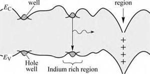
Other possible explanations for high radiative rates in III-V nitrides are the compositional alloy fluctuations, alloy clustering effects, and phase separation effects that necessarily result in a variation of the bandgap energy and lead to local potential minima, which carriers are attracted to and could be confined to (Nakamura and Fasol, 1997; Chichibu et al., 1996; Narukawa et al., 1997a, b). This explanation would be particularly suitable for ternary and quaternary alloy semiconductors such as GaInN and AlGaInN. The potential minima attract and confine carriers and prevent them from diffusing towards the dislocation lines. A band diagram showing energy - gap fluctuations and carrier localization is schematically illustrated in Fig. 13.11.
|
|
|
Fig. 13.11. Band diagram of GaInN having clusters of In rich regions which spatially localize carriers and prevent them from diffusing to dislocations. |
|
Electron Dislocation |
Because the direct detection of indium-composition fluctuations in GaInN by transmission - electron microscopy was shown to be difficult and even ambiguous due to high-energy electron - beam induced damage, the magnitude of the indium fluctuations in GaInN is still under discussion (Smeeton et al., 2003).
Recently, Hangleiter et al. (2005) pointed out that a reduction of GaInN/GaN quantum-well thickness occurs in the vicinity of V-shaped defects of III-V nitride epitaxial layers. The authors proposed that the higher bandgap energy associated with the thinner GaInN quantum wells shields the dislocation line-defect from mobile carriers located in the thicker (planar) GaInN quantum wells. As a result, a high radiative efficiency would be maintained in quantum-well structures despite the presence of dislocation line-defects. However, this model cannot explain the high radiative efficiency of GaN thin films.
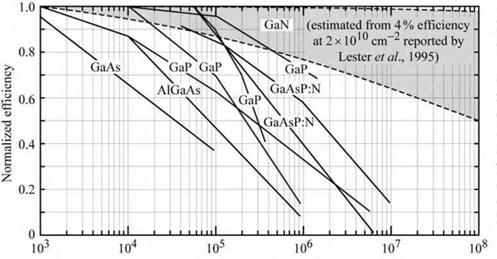
Although a generally accepted explanation has not yet been established, it remains a fact that the radiative efficiency in III-V nitrides, in particular GaInN/GaN blue emitters, exhibits low sensitivity to the presence of dislocations. That is, high radiative efficiencies are obtained in GaInN/GaN blue emitters despite high dislocation densities. This is illustrated in Fig. 13.12 which compares the normalized efficiency of different III-V semiconductors as a function of the
dislocation density in GaAs, AlGaAs, GaP, and GaAsP. Lester et al. (1995) estimated a 4% radiative efficiency for GaN with a dislocation density of 1010 cm-2. The shaded region is the estimation of the author of this book based on blue GaInN/GaN emitters. The data shown in the figure elucidate that III-V nitrides have a much higher tolerance towards dislocations as compared to III-V arsenides and phosphides.
|
|
|
Fig. 13.12. Dependence of radiative efficiency on etch pit density (III—V arsenide and phosphide data adopted from Lester et al., 1995; 11 I—V nitride data estimated by the author of this book based on data published by Lester eta!., 1995). |
|
Etch pit density (cm 2) |


 Опубликовано в