Total internal reflectors
 25 марта, 2014
  admin
admin Total internal reflection is a fascinating phenomenon occurring at the boundary between two dielectric media with different refractive indices. Total internal reflection was first discovered by Johannes Kepler in the early 1600s (Kepler, 1611). Kepler attempted to explain the apparent bending of objects partially submersed in water. Kepler discovered that for rays near normal incidence, the ratio of the angles of incidence and refraction is proportional to the ratio of what are now known as the refractive indices of the media. Kepler’s relationship can be expressed as
n101 = n2 02 (10 7)
where the angles 01 and 02 are measured with respect to the surface normal. Comparison with the law discovered between 1621 and 1625 by Cornelius Willebrord Snell (Snell’s law)
n^sin 0! = П2 sin 02 (10.8)
|
Fig. 10.4. Reflected and refracted light ray at the boundary between two media with refractive indices /7, and nl4 where /7 j > n1. |
|
n2 1 |
02 |
'— Refracted beam |
||
|
n |
Incident — beam |
y/vy |
— Reflected beam |
|
|
Kepler also discovered that, with suitable materials and sufficiently shallow angles of incidence, the refracted angle can be made to exceed 90°, resulting in total internal reflection. The critical angle for total internal reflection can be derived from Snell’s law using the condition 02 = 90°. Hence 01 crit = arcsin(n2/Щ) . (10.9) |
reveals that Kepler found the small-angle approximation of Snell’s law. The angles used in Snell’s law are shown in Fig. 10.4.
Because the ratio of the refractive indices on the right-hand side of the equation, n2 /n1, must be < 1.0, total internal reflection can occur only in the optically denser material. Total internal reflection occurs for all angles of incidence 91 > 01; crit. For grazing angles of incidence and a sufficiently high index contrast, a light ray cannot leave a medium of high refractive index.
Isaac Newton later showed that, for most transparent media, the refractive index could be taken as unity plus a term proportional to the medium’s mass density (measured in units of g /cm3). Media with high refractive index are therefore frequently called optically dense materials.
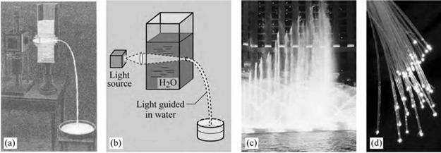
The most fascinating application of total internal reflection is fiber optic communication in which light rays, by undergoing total internal reflection events, are guided over thousands of kilometers in the core of a silica fiber. In 1841, the guiding of light was first demonstrated by Daniel Colladon using a jet of water as the high-index material (Hecht, 2001). This phenomenon is used to the present day to enhance the appearance of water fountains at night. The apparatus built by Daniel Colladon, who is considered the father of light guiding, is shown in Fig. 10.5.
|
Fig. 10.5. (a) Historical drawing and (b) schematic illustration of apparatus used in 1841 by Swiss engineer Daniel Colladon to demonstrate the guiding of light by total internal reflection in a jet of water, (c) Light guiding used to beautify appearance of fountain in Las Vegas, Nevada, (d) Fiber-optic strands (after TheFreeDictionary. com, 2005). |
In light-emitting devices based on semiconductors, total internal reflection represents a major problem as it hinders the out-coupling of light out of the semiconductor die. As semiconductors have a large refractive index of typically 2.0-3.5, the critical angle for total internal reflection is small. Whereas the problem is severe for III-V arsenides and phosphides (n * 3.0) it is less
severe for III-V nitrides (n * 2.0). Total internal reflection is of little concern in organic light-
emitting diodes due to the low refractive indices of organic materials.
|
|
|
Ag/Air: R = 98.5% (Ag/GaAs: R = 96%) |
|
. GaAs/AlGaAs/AIAs |
|
J і і і i L_i. |
One of the unique features of total internal reflection is that the magnitude of the reflection is R = 1.0 (“total”). This enables the demonstration of reflectors with zero mirror loss, a feature that has been employed advantageously in lasers. Edge-emitting lasers (Smith et al., 1993) as well as microdisk lasers (“whispering gallery lasers”) (McCall et al., 1992) have employed total internal reflection to demonstrate cavities with very high cavity-quality factors.
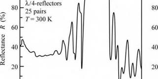
Fig. 10.6. Reflectance of a silver/air rcflector and a 25-pair AlAs/GaAs distributed Bragg reflector (DBR).
j_________ і_____ і і ~~1
0.6 0.7 0.8 0.9 1.0 0.6 0.7 0.8 0.9 1.0 1.1
Wavelength X (ціп) Wavelength X (цш)
10.1 Distributed Bragg reflectors The reflectance spectra of a metal mirror and a DBR are compared in Fig. 10.6. Whereas metal reflectors exhibit a broad band with high reflectivity, DBRs display only a narrow band of high reflectivity denoted as the stop band. However, while the metal reflector has a certain reflectivity, the DBR’s reflectivity can be increased by increasing the number of reflector pairs so long as these reflector pairs are fully transparent.
For LED structures on light-absorbing substrates, about 50% of the light emitted by the active region is absorbed by the substrate. This represents a substantial loss. The absorption of light in the substrate can be avoided by placing a reflector between the substrate and the LED active layers. Light emanating from the active region towards the substrate will then be reflected and can escape from the semiconductor through the top surface.
Distributed Bragg reflectors (DBRs) are well suited for inclusion between the substrate and the active layers. The schematic LED structure with a DBR is shown in Fig. 10.7. LEDs with DBRs were first demonstrated by Kato et al. (1991) in the AlGaAs/GaAs material system. The LED had a 25-pair AlAs/GaAs or AlGaAs/GaAs DBR and emitted in the infrared at 870 nm.
|
|
A DBR is a multi-layer reflector consisting of typically 5-50 pairs of two materials with different refractive indices. As a result of the difference in refractive index, Fresnel reflection occurs at each of the interfaces. Usually the refractive index difference between the two materials is small so that the magnitude of the Fresnel reflection at one interface is also quite small. However, DBRs consist of many interfaces. More importantly, the thicknesses of the two materials are chosen in such a way that all reflected waves are in constructive interference. For normal incidence, this condition is fulfilled when both materials have a thickness of a quarter wavelength of the light, i. e.
tlh = ^lh/4 = X0 / (4 nlh) (normal incidence) (10.10)
where X0 is the vacuum Bragg wavelength of the light, tl;h is the thickness of the low-index (l) and high-index (h) material, and nlh is the refractive index of the low-index (l) and high-index
(h) material. The thickness of tl;h given in Eq. (10.10) can be not only X/4, but also an odd - numbered integer multiple of X /4, i. e. 3X /4, 5X /4, 7X /4, and so on. These thicknesses will also result in constructive interference of the reflected waves. For layer thicknesses greater than X /4, e. g. 3X /4, the reflector will, however, have a narrower high-reflectivity stop band.
For an oblique angle of incidence, the wave vector can be separated into a parallel and a normal component. As in the normal-incident case, the thickness of the DBR layers must be a quarter wavelength for the wave vector component normal to the DBR layers. For an oblique angle of incidence ©l;h, the optimum thicknesses for high reflectivity are given by
tlh = Xjh/(4cos©lh) = X0/(4щh cos©lh) (oblique incidence) . (10.11)
Again, the thickness tl;h given in Eq. (10.11) can also be an odd-numbered integer multiple of the value given by the equation. For DBRs with sufficiently many quarter-wave pairs, reflectivities
near 100% can be obtained.
A DBR must fulfill several additional conditions. Firstly, since a DH is usually grown on top of the DBR, the DBR must be lattice matched to the DH in order to avoid misfit dislocations. Secondly, to attain high-reflectivity DBRs, the constituent DBR materials need to be transparent at the wavelength of operation unless the DBR has a high index contrast. High index-contrast DBRs (e. g. Si/SiO2) yield high reflectivity, even if one of the materials is weakly absorbing at the wavelength of interest. Thirdly, if the DBR is in the current path, the DBR must be conductive.
|
|
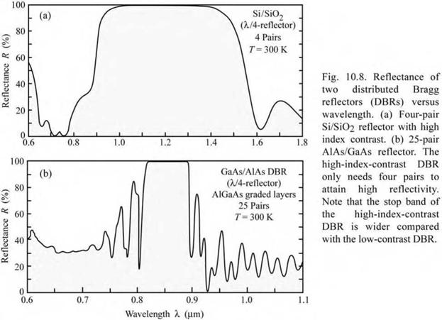
The reflectances of a Si/SiO2 and an AlAs/GaAs DBR versus wavelength are shown in Fig. 10.8. The Bragg wavelength is located in the center of the high-reflectivity band or stop band. Inspection of the figure reveals that (/) the reflectivity of high-contrast DBRs (Si/SiO2) is much higher than the reflectivity of low-index-contrast DBRs (AlAs/GaAs) for the same number of quarter-wave pairs and that (if) the width of the stop band of the high-index - difference DBR is much wider than the stop band width of the low-contrast DBR.
Properties of DBRs can be calculated by the matrix method (Born and Wolf, 1989). The properties of DBRs have been analyzed in detail by Coldren and Corzine (1995), Yariv (1989), and Bjork et al. (1995). Here, only a brief summary will be given.
Consider a distributed Bragg reflector consisting of m pairs of two dielectric, lossless materials with refractive indices nl and nh. The thicknesses of the layers are assumed to be a quarter wave, i. e. Ll = XBragg / (4 nl), and Lh = XBragg / (4 nh). The period of the DBR is Ll + Lh. The reflectivity of a single interface is given by Fresnel’s equation for normal incidence
r = . (10.12)
-h + -1
Multiple reflections at the interfaces of the DBR and constructive interference of the multiple reflected waves increase the reflectivity with increasing numbers of pairs. The reflectivity has a maximum at the Bragg wavelength XBragg. The reflectivity at the Bragg wavelength of a DBR with m quarter-wave pairs is given by (Coldren and Corzine, 1995)
|
1 - (/ - h )2m 1 + ( / - h )m |
|
D I |2 ^DBR = rDBR |
|
(10.13) |
The stop band of a DBR depends on the difference in refractive index of the two constituent materials, nh - nl = A—. The spectral width of the stop band is given by (Yariv, 1989)
2 XBragg A—
AX stopband = — (10.14)
neff
where —eff is the effective refractive index of the DBR. For efficient operation of the LED, the
stop band should be wider than the emission spectrum of the active region.
The effective refractive index of the DBR can be calculated by requiring the same optical path length normal to the layers for the DBR and an effective medium. The effective refractive index is then given by
r 1 1 ^-1
—eff = 2 — + — . (10.15)
I nl —h J
For small index differences, i. e. A— <<A—l, the effective refractive index can be
approximated by
The optical wave penetrates into the DBR only by a finite number of quarter-wave pairs. That is, a finite number out of the total number of quarter-wave pairs are effectively reflecting the wave. The effective number of pairs “seen” by the wave electric field is given by (Coldren and Corzine, 1995)
|
nh - n1 ^ nh + Щ |
|
± _Пк±П_ tanh 2 n^ - n |
|
(10.17) |
|
2m |
|
meff |
|
(10.18) |
For thick DBRs (m ^ да), the tanh function approaches unity and one obtains
meff * — - r
2 nh - n1
|
|
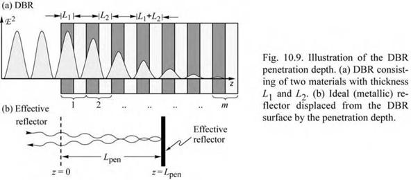
At the Bragg wavelength (X = XBragg), the phase change of the reflected wave is zero. In the vicinity of the Bragg wavelength (X * XBragg), the phase of the reflected wave changes linearly with wavelength. It is therefore possible to approximate a DBR with a metal-like mirror located a distance Lpen behind the first dielectric interface, as shown in Fig. 10.9. The reflection of the DBR can thus be expressed as
rDBR - I'DBlR e-2i<в - )Lp'" (10.19)
where в = 2п / X is the average phase constant of the wave. The phase change at z = 0 (see
Fig. 10.9) of the wave reflected by the metal mirror is given by
rmetallz =0 = |r,«al|e2i(2’A)Lp“ . (10.20)
Equating the phase changes given by Eqs. (10.19) and (10.20) and using the phase changes of a
DBR (Coldren and Corzine, 1995), the penetration depth is given by
Lpen = L +L2 tanh (2mr) . (10.21)
v 4r
For a large number of pairs (m ^ да), the penetration depth is given by
L - L1 +L = (L1 +L) ”h +” . (10.22)
pen 4 r 4 nh - nl
Comparison of Eqs. (10.22) and (10.18) yields that
Lpen = (1/2) meff (L: + L2) . (10.23)
The factor of (1/2) in Eq. (10.23) is due to the fact that meff applies to the effective number of periods seen by the electric field, whereas Lpen applies to the optical power. The optical power is equal to the square of the electric field and hence it penetrates half as far into the mirror. The effective length of a cavity consisting of two DBRs is thus given by the sum of the thickness of the center region plus the two penetration depths into the DBRs. The effective length of a cavity with DBRs is thus longer than the effective length of a cavity with metal mirrors.
The reflectivity of the DBR depends on the polar angle of incidence and on the wavelength. Although an analytic result can be obtained for the reflectivity of a DBR at the Bragg wavelength for normal incidence, the reflectivity of a DBR at an arbitrary wavelength and an arbitrary angle of incidence can only be calculated numerically. If light from an isotropic source is reflected by a DBR, the reflected intensity can be obtained by integration over all angles. The angle-integrated reflectance at a certain wavelength X is then given by
|
|
The total light intensity reflected by the DBR is calculated by
|
(10.25) |
Ir = fX Ii(X)Rint(X)dX
where Ii(X) is the emission intensity spectrum of the active region incident on the DBR and Ir is the intensity reflected by the DBR. For an isotropic emitter such as the active region of an LED, it can be assumed that the emission spectrum incident on the DBR is independent of the emission angle.
An efficient DBR will be optimized in such a way that it maximizes the intensity of the reflected light. In addition, the escape of the light reflected by the DBR from the LED die must be taken into account. Maximizing the LED extraction efficiency using a DBR is a complicated problem that cannot be solved analytically. Ray tracing computer software is used to maximize the extraction efficiency in LED structures with DBRs.
A priori, it is not clear that the use of conventional DBRs provides the best extraction efficiency. DBRs with layer thicknesses thinner or thicker than a quarter-wave should also be considered for maximization of the extraction efficiency. Such variable-thickness DBRs have a lower reflectivity but a wider stop-band width compared with quarter-wave DBRs. For active regions with broad emission spectra, such variable-period DBRs can be advantageous.
Ideally, the layers comprising the DBR are transparent. Layers of transparent DBRs have negligible absorption losses. However, transparent materials may not always be available so that absorbing materials must be used. Such absorbing DBRs have a maximum reflectivity of less than 100%, even if an infinite number of pairs are used.
An example of a partially absorbing Si/SiO2 DBR is shown in Fig. 10.8. Silicon absorbs light for X < 1.1 ^m, i. e. for hv > Eg. However, the results shown in the figure demonstrate that very high reflectivities can be attained at 1.0 ^m, where Si is absorbing. This is due to the high index contrast between Si and SiO2.
Transparent and absorbing DBRs lattice matched to GaAs are used in the AlGaInP/GaAs material system. This material system is used for high-efficiency visible LEDs emitting at X > 550 nm (green, yellow, amber, orange, and red). The properties of transparent and absorbing
DBRs used in this material system have been compiled by Kish and Fletcher (1997) and are summarized in Table 10.3. Inspection of the table reveals that the absorbing Al05In05P/GaAs DBRs have the advantage of a high refractive index contrast. However, the absorbing nature of the DBR imposes an upper limit on the maximum reflectivity. High-contrast DBRs have a wider stop-band width. The transparent Al05In0.5P/(AlGa)0.5In05P DBRs have the advantage of negligible optical losses. However, many pairs are needed to attain high reflectivity and the stopband width is narrower than in high index-contrast DBRs.
|
Table 10.3. Properties of distributed Bragg reflector (DBR) materials used for visible and infrared LED applications. The DBRs marked as “lossy” are absorbing at the Bragg wavelength (data after Adachi, 1990; Adachi et al., 1994; Kish and Fletcher, 1997; Babic et al, 1999; Palik, 1998).
|
In practice, transparent layers are used at and near the top (epitaxial side) of the DBR whereas absorbing layers are used towards the bottom (substrate side) of the DBR. For DBRs used in manufactured AlGaInP/GaAs LEDs, each of the layers is different and optimized to keep the number of pairs low, the absorption low, and the reflectivity spectrum broad (Streubel, 2000).
Table 10.3 also shows properties of the AlAs/GaAs and the SiO2/Si material systems. The SiO2/Si material system is an example of a high index-contrast system. However, it cannot be used for current conduction due to the insulating nature of the SiO2. The AlAs/GaAs material system is used in resonant-cavity LEDs and vertical-cavity surface-emitting lasers emitting in the range 880-980 nm.
A DBR that is resonant with the peak-emission wavelength, is not necessarily the optimum reflector for an absorbing substrate (AS) LED. Although a DBR has a high reflectivity for normal incidence, it rapidly decreases for off-normal angles of incidence. Assume that the angle of incidence is 9 = 0° at normal incidence. Since the solid angle (per angle interval d9) increases
|
|
|
with angle 9 according to a sine function, it is advantageous to shift the normal-incidence resonance wavelength of the DBR to wavelengths longer than the peak emission wavelength. |
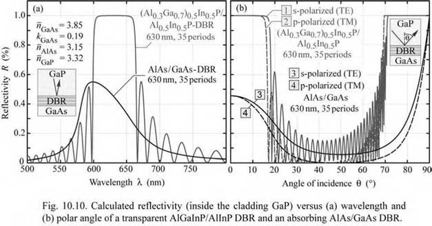
The calculated reflectivities of a transparent and an absorbing DBR versus wavelength and polar angle of incidence are shown in Fig. 10.10. Whereas the DBR made of the transparent materials has a reflectivity close to 100% at the Bragg wavelength, the DBR that includes the absorbing GaAs layers has a maximum reflectivity of about 55%. This value cannot be increased by adding additional pairs to the DBR, because the limitation of the value lies in the absorptive nature of the DBR. The figure also shows the reflectivity of the DBRs versus the angle of incidence. Inspection of the figure reveals a major drawback of DBRs, namely the limitation of the high reflectivity band to small angles of incidence. For angles of incidence greater 20°, the reflectivity strongly decreases to assume values close to zero. Thus, for oblique angles of incidence (20° < 9 < 70°), the DBR becomes non-reflective. The lack of reflectivity is a major loss mechanism in AlGaInP LEDs whose active layers are grown on top of a DBR that in turn is located on the absorbing GaAs substrate.
Next a formula will be derived that gives the critical angle, 0c, at which the reflectivity of a DBR strongly decreases. The structure of a DBR and the critical angle are illustrated in Fig. 10.11 (a) and (b), respectively. Note that the outside medium is a semiconductor with refractive index n0. For normal incidence (0 = 0°), the Bragg condition is fulfilled at the Bragg
wavelength, XBragg, which is located at the center of the high-reflectivity stop band. The Bragg wavelength shifts with angle of incidence, as shown in Fig. 10.11 (c). However, the width of the stop band does not depend on the angle of incidence as long as it is small. We can thus write the following condition for the critical angle 0c
AXBragg — XBragg(0 — 0 ) — XBragg(0c) — 1 AXstopband. (1°.26)
|
ragg |
|
|
|
о Э>0°/ Ґ |
|
Y=o° ' V Л S- |
|
(a) |
(b) |
R (c) |
|
I®/ |
||
|
A |
||
|
«11 |
||
|
f>2 |
||
|
L 0 |
|
R 0: |
|
0c |
|
Fig. 10.11. (a) DBR stucture used in calculation, (b) Reflectivity versus angle of incidence and critical angle at which reflectivity decreases, (c) DBR reflectivity versus wavelength for two angles of incidence. |
Using the expression for the angle-dependent Bragg wavelength and the expression for the width of the stop band given earlier in this chapter, one can write
|
fH0.0 A c |
|
An |
|
1 |
|
XBragg(0 - 0°) |
|
(10.27) |
|
1 - cos |
|
n + n2 n0 |
|
n1 |
|
J. |
|
- 2 XBragg (0 - 0°) |
Dividing both sides of the equation by XBragg(0 = 0°) and solving the equation for 0c yields
|
|
(10.28)
Using the approximation cos x « 1 - (1/2) x2 (valid near x = 0) and arcos x « [2 (1 - x)]1/2 (valid
|
|
near x = 1), the following approximation is obtained
(10.29)
The equation shows that the critical angle strongly depends on the refractive index of the outside medium, n0, with 0c к (w0)-3/2 Thus the critical angle is small for outside media with a high
refractive index. For this reason, it is difficult if not impossible to attain omnidirectional
reflection characteristics with a DBR if the outside medium is a high-index semiconductor.
As a numerical example, we consider an AlAs/GaAs DBR (nAlAs= 3.0; nGaAs= 3.5) with
GaP as the outside medium (nGaP = 3.1). Insertion of these values in the equation for the critical
angle yields 0c = 20.5°, which is relatively close to normal incidence. Even high-contrast DBRs, such as SiO2/Si DBRs, do not have omnidirectional characteristics if the outside medium is a high-index semiconductor.
Different strategies have been employed to optimize DBRs. Chiou et al. (2000) used a composite DBR in an AlGaInP LED, that is, two types of DBRs stacked on top of each other, namely a non-absorbing (Al0.4Ga0.6)0.5In0.5P/Al0.5In0.5P DBR resonant at the peak emission wavelength of 590 nm and an additional high-contrast absorbing AlAs/GaAs DBR. This DBR was located below the phosphide DBR. The arsenide DBR was resonant at a wavelength about 10% longer than the peak emission wavelength in order to reflect light incident at off-normal angles. The authors found a substantial improvement in light output with the composite DBR.
Non-periodic DBRs have a wider stop band and thereby a high reflectivity over a wider range of angles. To find optimum non-periodic DBR structures, numerical simulations and optimization procedures have been conducted (see, for example, Li et al., 1999).
As shown by the calculation above, an increase in index contrast will provide a wider range of angles within which a high reflectivity is maintained. The use of such high-contrast DBRs in LEDs has been proposed by Chiou et al. (2003) who disclosed the use of an AlGaAs/AlxOy DBR in an LED. Al2O3 has a refractive index of about 1.75 whereas Al-rich AlGaAs has a refractive index of about 3.25 thus providing a large index contrast of An = 1.5. The AlxOy layers of the DBR were fabricated from epitaxially grown AlAs by using an oxidation process that is performed in water vapor at temperatures of 400-450 °C. The AlxOy layers of the DBR are not conductive thus necessitating non-oxidized AlAs openings in the AlxOy layers, which provide a current path between substrate and active layers.
DBRs can have a high electrical resistance for current transport perpendicular to the layers. The resistance can pose a substantial problem in LED and laser structures, which manifests itself in a high forward voltage. Early experiments on VCSELs or vertical-cavity surface-emitting lasers (Jewell et al., 1989; Koyama et al., 1989) revealed forward voltages as high as 30.0 V (Jewell, 1992) and prevented these first devices from lasing in continuous-wave mode. The high resistance is caused by abrupt heterojunctions which pose barriers for carrier transport. Fortunately, heterojunction barriers can be completely eliminated by parabolic compositional grading (Schubert et al., 1992a, 1992b). Such compositional grading is now routinely used in




 Опубликовано в