Theory of temperature dependence of diode forward voltage
 16 марта, 2014
  admin
admin The derivation of the temperature dependence of the forward voltage presented here follows the analysis first given by Xi et al. (2004; 2005). The I-V characteristic of an ideal p-n junction diode is given by the Shockley equation
6.3 Theory of temperature dependence of diode forward voltage
|
e Vf /(nidealkT) |
|
(6.3) |
|
- 1 |
|
J = Js (e |
where Js is the saturation current density. For non-degenerate semiconductors and under forward bias conditions, Vf >> kT / e, one obtains
|
nidealkT |n С Jf 1 |
|
df d T |
|
d dT |
|
(6.4) |
|
V Js J |
|
e |
The saturation current density depends on the diffusion constants of electrons and holes, the lifetimes of electrons and holes, the effective density of states at the conduction band and valence band edges, and the bandgap energy, all of which depend on the junction temperature. The
3/2 •
temperature dependence of the effective density of states is given by Nc, v к T. Assuming
phonon scattering, the temperature dependence of the carrier mobility is д к T 3/2. Using the
1/2
Einstein relation, the diffusion constant depends on temperature according to D к T~ . The minority carrier lifetime can either decrease (non-radiative recombination) or increase (radiative recombination) with temperature. Due to this uncertainty, the minority carrier lifetime is assumed to be independent of temperature. Using these temperature dependences in Eq. (6.4) and executing the derivative yields
|
d Vf ~dT |
|
3k |
|
(6.5) |
|
eT |
|
e |
|
eVf - Eg і dEg |
|
e d T |
This equation gives the fundamental temperature dependence of the forward voltage. The first, second, and third summands on the right-hand side of the equation are due to the temperature dependence of the intrinsic carrier concentration, bandgap energy, and effective densities of states, respectively. The equation includes the temperature dependence of the bandgap energy, which had not been taken into account in earlier derivations of dVf / dT (Millman and Halkias, 1972).
LEDs are typically operated at forward voltages close to the built-in voltage, i. e. Vf ~ Vbi. Thus, for non-degenerate doping concentrations, we can write
|
С Nd Na л n2 |
|
С Nc Nv ^ |
|
С Nd Na 1 v Nc Nv j |
|
eVf - Eg « kT ln |
|
- kT ln |
|
= kT ln |
|
(6.6) |
|
v ni |
|
1_ |
GaN |
і 1 |
i = 7 A |
|||
|
1 |
Li |
|||||
|
1 1 |
||||||
|
1 U о |
||||||
|
■ t |
0 m 0 і |
. .. |
|
3.5 J.4 |
|
bo |
|
a. я 1 ЗЛ Я CQ |
|
200 |
|
400 |
|
600 |
|
*------ 1 |
i 1 1 |
|||||
|
GaP |
I 1 1 |
|||||
|
1 |
g = 2.27 eV |
|||||
|
1 о |
||||||
|
о СП 1 ____ 1___ |
____ |
|
200 |
|
400 |
|
600 |
|
800 |
|
> О |
|
з.°0- 1.6 |
|
1000 |
|
GaAs |
i 1 1 |
|||||||
|
,= 1.4 |
24 eV |
|||||||
|
InP |
__ і |
|||||||
|
' -£ l |
g= 1.35 eV" |
|||||||
|
■"IT |
1 ------- U^_£g= 1.12 eV |
1— |
s. V. |
|||||
|
1 1 |
||||||||
|
1 1 U |
||||||||
|
о о ГО 1 |
||||||||
|
Ge |
1 1 _ 1 |
|||||||
|
^£g = 0.66 eV і |
||||||||
|
1 1 і |
|
1.5 1.4 1.3 |
|
> -2d- 1.2 |
|
Uj 1.1 С u 1.0 c. C3 ti) с 0.9 cs a |
|
0.8 0.7 0.6 0.5 |
|
2 0 800 z‘u0 |
|
0 200 400 600 Temperature T (K) |
|
800 |
|
2.5 2.4 2.3 2.2 2.1 |
|
£g(0K) |
«(Ю-4^) |
P(K) |
|
|
GaN |
3.470 |
7.70 |
600 |
|
GaP |
2.340 |
6.20 |
460 |
|
GaAs |
1.519 |
5.41 |
204 |
|
InP |
1.425 |
4.50 |
327 |
|
Si |
1.170 |
4.73 |
636 |
|
Ge |
0.744 |
4.77 |
235 |
|
Varshni formula: £ = £ (OK) - |
|
g |
|
аГ 7" + p |
|
Fig. 6.4. Fundamental bandgap energy of GaN, GaP, GaAs, InP, Si, and Ge as a function of temperature. The bandgap energy is approximated by the Varshni formula which uses the fitting parameters a and P (from data compiled by Ioffe, 2004). |
|
|
The second summand on the right-hand side of Eq. (6.5) is due to the changes in bandgap energy. As the temperature increases, the energy gap of semiconductors generally decreases. The temperature dependence of the energy gap of a semiconductor can be expressed by the Varshni formula (Varshni, 1967)
(6.7)
where a and в are fitting parameters, frequently called the Varshni parameters. The bandgap energy versus temperature for several semiconductors is shown in Fig. 6.4 along with the values
for a and p. The Varshni parameters for several semiconductors, compiled by the Ioffe (2004), are given in Table 6.1. Substituting Eqs. (6.6) and (6.7) into Eq. (6.5) yields
|
dVf k —— « — ln d T e і |
С NDNA '1 a T (T + 2 P) 3k VNc NvJ e(T + P)2 e |
|
due to T 1 dEg due to T dependence dependence of ni e dT of DOS |
This equation is a very useful expression for the temperature coefficient of the forward voltage.
|
Table 6.1. Varshni parameters of common semiconductors (from data compiled by Ioffe, 2004).
|
For GaN diodes, Xi et al. (2004; 2005) reported a calculated dVf /dT of -1.76 mV/K, which is in good agreement with the experimental value of -2.3 mV/K. Deviations between theory and experiment were attributed to the temperature coefficient of the resistivity in the neutral regions which decreases with increasing temperature due to a higher doping activation (Xi et al., 2005).
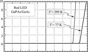
The temperature dependence of a GaPAs/GaAs LED is illustrated in Fig. 6.5, which shows the I-V characteristic at 77 K and at room temperature. Inspection of the figure reveals that the threshold voltage as well as the series resistance of the diode increases as the diode is cooled. If the device were driven at a constant voltage, e. g. 1.9 V, a large current change would result from the change in temperature.
|
|
|
-2-10 1 2 Voltage V (V) |
|
Fig. 6.5. Current—voltage characteristic of GaAsP/GaAs LED emitting in the red part of the visible spectrum, measured at 77 and 295 K. The threshold voltages are 2.0 and 1.6 V, at 77 and 300 K, respectively. |
Exercise: Temperature dependence of diode forward voltage. Experimentally determined linear temperature coefficients (dVf / dT) for GaAs diodes range from 1.2 to 1.4 mV/K. Calculate the linear temperature coefficient of the forward voltage of a GaAs diode with NA = ND = 2 x 1017 cm-3 at room temperature. What is the decrease in forward voltage if the ambient temperature is increased from 20 to 40 °C and the internal heating in the diode can be neglected?
Solution: For GaAs with a = 5.41 x 10⁻⁴ eV/K and p = 204 K, one obtains at room temperature dVf / dT = - 1.09 mV/K. The decrease in diode voltage for the 20 °C temperature increase is AVf =
21.9 mV.
|
Device in oven |
|
Oscilloscope
|
|
/ |
(a) Calibration Pulse generator
(b) Junction temperatue measurement DC current source Device in 20 °С ambient
I2D
Fig. 6.6. (a) Pulsed calibration procedure establishing the forward voltage versus junction temperature (Kf versus 7]) relation and (b) determination of junction temperature for different DC forward currents.
6.4 Measurement of junction temperature using forward voltage This method consists of a Vf calibration measurement under pulsed-current injection, and a Vf measurement under DC-current injection. The two measurements are illustrated in Fig. 6.6. In the calibration measurement, the device under test is located in a temperature-controlled oven, so that the temperature of the device and junction is known. The temperature is varied from typically 20 °C to 120 °C. The calibration measurement is performed in a pulsed mode with a
very small duty cycle (e. g. 0.1%), so that the heat generated by the injection current becomes negligibly small. The forward voltage is measured at each temperature for the current levels of interest. The calibration measurement establishes the relation between forward voltage and junction temperature for the If levels of interest.
|
|
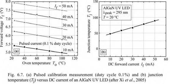
Subsequently the device is exposed to room-temperature ambient and subjected to a series of DC currents. Forward voltages are measured once thermal steady state has been reached. The measured DC forward voltages and the calibration measurement data are used to establish the junction temperature for different current levels. A calibration measurement and a junction temperature measurement for an AlGaN deep UV LED is shown in Fig. 6.7 (Xi et al., 2005).
Junction temperatures of several different devices are shown in Fig. 6.8 including red (AlGaInP, X = 625 nm), green (GaInN, X = 525 nm), blue (GaInN, X = 460 nm), and UV (GaInN, X = 370 nm) devices packaged in conventional 5 mm packages (Chhajed et al., 2005). The forward-voltage method is accurate to within a few degrees. The Vf method is more accurate than the peak-wavelength method. The latter method is limited by the uncertainty in the peak wavelength, which is difficult to determine accurately for broadened emission bands. Also shown in the figure is the carrier temperature derived from the high-energy slope of the spectrum. The accuracy of the carrier temperature suffers from alloy broadening, which decreases the high-energy slope (and thus increases the apparent carrier temperature).
|
:(a) GalnN UV LED, High energy slope к |
||||
|
■ ~°_ л peak |
||||
|
■ Tcarrier- |
||||
|
Accuracy |
||||
|
: t |
= 20 |
’C |
-ф_± -Ф-±10С |
С С' |
|
270 210 150 90 30 900 700 500 300 100 |
|
p <u o. |
|
. (с} GalnN preen |
LED |
|||
|
■ Accuracy -Л - + Ч °С |
||||
|
.А |
||||
|
-Ф - і 15 °С |
||||
|
• |
1 л |
^carrier ■ |
||
|
т=: |
!() °С |
|||
|
■.................................................. |
|
0 20 40 60 80 100 DC current I (mA) |
|
:(b) GalnN ■ Accuracy : _ф_± 3 °С : -4- + 1S °С |
blue |
LED |
|||
|
--- .--- |
--- •-- |
T- ■ |
= 20° --- .-- |
С : |
|
|
^(d) AIGah ■ Accuracy L + i °r |
P red LED |
--- — |
- |
||
|
:-ф-± |
5 °С |
ґ ^carrier |
|||
|
= 20° |
c ■ |
||||
|
r= |
|
Fig. 6.8. Junction and carrier temperature of devices in conventional 5 mm packages as a function of DC injection current. The measured carrier temperature over-estimates the true carrier temperature due to alloy broadening (after Chhajed et al., 2005). |
|
0 20 40 60 80 100 DC current / (mA) |
6.5 Constant-current and constant-voltage DC drive circuits Different considerations play a role in designing the DC drive circuit of an LED operated under steady-state conditions. These considerations include the simplicity and cost of the drive circuit, the power efficiency, and the compensation of the temperature dependence of the light intensity emitted from the LED.
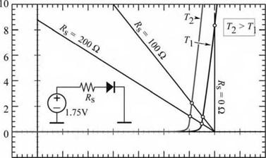
A simple drive circuit is a constant-voltage supply such as a battery or the rectified AC output of a transformer. There are, however, two drawbacks to constant-voltage drives of LEDs. Firstly, the diode current depends exponentially on the voltage, so a small variation in the drive voltage results in a large change in the current. Secondly, the threshold voltage of a diode depends on temperature, so any temperature change results in a significant change in current. A constant-voltage operating characteristic of a diode is shown in Fig. 6.9.
If a resistor is connected in series with the diode, the strong temperature dependence of the diode current is reduced. The series resistance together with the temperature dependence of the diode determines the temperature coefficient of the diode current.
When a diode is driven with a constant current, the emission intensity decreases with increasing temperature. A constant-voltage power supply with a series resistance can be used to reduce the temperature dependence of the emission intensity. The emission intensity of LEDs generally decreases with increasing temperature due to non-radiative recombination. In addition, the threshold voltage decreases with increasing temperature. However, for a constant-voltage supply, the diode current increases as the temperature increases, as shown in Fig. 6.9. Thus a
series resistor can be used to compensate for the emission intensity decrease at elevated temperatures. It should be noted that the electrical-to-optical power-conversion efficiency drops due to the power consumed in the series resistor.
|
|
|
Fig. 6.9. LED drive circuit with series resistance Rs- The intersection between the diode I-V characteristics and the load lines are the points of operation. Small series resistances result in an increased diode current at high temperatures, thus allowing for compensation of a lower LED radiative efficiency. |
|
Voltage V (V) |
|
0 0.5 1.0 1.5 2.0 |
The temperature dependence of LED intensity is an important factor for LEDs used in outdoor applications. On hot summer days, the temperature and the ambient light intensity are high. Owing to the high temperature, the LED intensity drops. In addition, high brightness is required due to high ambient light levels. This effect can be compensated for by driving the LEDs with a higher current as the temperature increases.
A constant-current drive circuit can consist of a transistor with the LED as a load. A constant-current drive circuit allows one to drive the LED irrespective of the diode threshold voltage and the diode temperature. However, a constant-current drive circuit does not compensate for the decrease of LED emission at elevated temperatures.
Exercise: Compensation of the temperature dependence of an LED with a drive circuit. Consider an LED with a characteristic temperature T1 = 100 K, a turn-on voltage of 1.4 V at 20 °C, a temperature coefficient of the turn-on voltage of -2.1 mV/K, and a linear I-V characteristic with a differential resistance of 5 Q for forward voltages larger than the turn-on voltage. Assume that the temperature
dependence of the emission intensity is given by I = I|300 K exp [ - (T - 300 K) / T1 ].
Design a drive circuit consisting of a constant-voltage source and a resistor, which compensates for the temperature dependence of the emission intensity of the LED so that the LED emission intensity is the same at the water freezing-point temperature (0 °C) and 60 °C. The LED should draw 20 mA at the freezing-point temperature.
Solution: At 60 °C, the current needs to be 36.4 mA in order to keep the emission intensity independent of temperature. Constructing a load line that intersects the 0 °C and 60 °C diode I-V characteristic at 20 mA and 36.4 mA, respectively, yields the following values for the drive circuit:
Constant-voltage source with V = 1.6 V and series resistance of 2.7 Q.


 Опубликовано в