Packaging
 26 марта, 2014
  admin
admin 11.1 Low-power and high-power packages Virtually all LEDs are mounted in a package that provides two electrical leads, a transparent optical window for the light to escape, and, in power packages, a thermal path for heat dissipation. The chip-encapsulating material advantageously possesses high optical transparency, a high refractive index, chemical inertness, high-temperature stability, and hermeticity. The refractive index contrast between the semiconductor and air is reduced by including an encapsulant thereby increasing the light extraction efficiency. Virtually all encapsulants are polymers with a typical refractive index of 1.5 to 1.8. A reduced index contrast at the semiconductor surface increases the angle of total internal reflection thereby enlarging the light escape cone and the extraction efficiency.
|
|
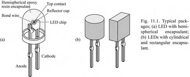
A low-power package is shown in Fig. 11.1 (a). The active device is die-bonded or soldered to the bottom of a cup-like depression (“reflector cup”) in one of the lead wires (usually the cathode lead). A bond wire connects the LED top contact to the other lead wire (usually the
anode lead). The LED package shown in the figure is frequently referred to as a “5 mm” or “T1- 3/4” package.
|
|
In low-power LEDs, the encapsulant has the shape of a hemisphere, as shown in Fig. 11.1 (a), so that the angle of incidence at the encapsulant-air interface is always normal. As a result, total internal reflection does not occur at the encapsulant-air interface. There are types of LEDs that do not have a hemispherical shape for the encapsulant. Some LEDs have a rectangular or cylindrical shape with a planar front surface. Examples of such shapes are shown in Fig. 11.1 (b). Planar-surface LEDs are frequently used under circumstances where the intended viewing angle is close to normal incidence or where the LED is intended to blend in with a planar surface. Encapsulants provide protection against unwanted mechanical shock, humidity, and chemicals. The encapsulant also stabilizes the anode and cathode lead, the LED chip and bonding wire.
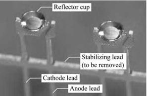
Fig. 11.2. Leadframe of a conventional 5 mm package for mounting and connecting LED chips. The stabilizing lead is cut off once mechanical stability between the anode and cathode lead has been established by the epoxy encapsulant.
A photograph of a series of LED leadframes is shown in Fig. 11.2. The individual leadframes are connected via a temporary stabilizing lead that is removed after die bonding, wire bonding, and the establishment of mechanical stability between anode and cathode lead by the epoxy encapsulant. The LED chip is die-bonded to the flat bottom of the highly reflective reflector cup with a silver-loaded electrically conductive epoxy being a common die-bonding material. Note that for power chips, metal-based solders are preferable as die-bonding materials due to their inherently lower thermal resistance compared with conductive epoxies.
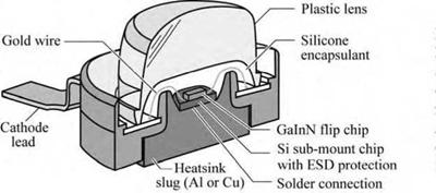
A power package is shown in Fig. 11.3. Power packages have a direct, thermally conductive path from the LED chip, through the package, to a heat sink, e. g. a printed circuit board. The power package shown in the figure has several advanced features. Firstly, the package contains an Al or Cu heatsink slug with low thermal resistivity to which the LED submount is soldered by a metal-based solder. Secondly, the chip is encapsulated with silicone. Because standard silicone
retains mechanical softness in its cured state, the silicone encapsulant is covered with a plastic cover that also serves as lens. Thirdly, the chip is directly mounted on a Si submount that
includes electrostatic discharge protection (ESD).
|
|
|
Fig. 11.3. Cross section through high-power package. The heatsink slug can be soldered to a printed circuit board for efficient heat removal. This package, called the Barracuda package, was introduced by Lumileds Corp. (adapted from Krames, 2003). |
Photographs of the high-power package are shown in Fig. 11.4 including a high - magnification micrograph, Fig. 11.4 (b), revealing interdigitated contacts of a GaN-based LED. Fig. 11.4 (c) shows the package soldered to a printed-circuit board that possesses high thermal conductivity for efficient cooling (LED Museum, 2003). Several light-emitting diodes located on a single chip may be interconnected in series to increase operating voltage and decrease operating current of a device (Krames et al., 2002, 2003).
|
Fig. 11.4. (a) High-power package; (b) LED die in package; (c) package on printed circuit board with high thermal conductivity ((a) after Krames, 2003; (b), (c) after after LED Museum, 2003). |


 Опубликовано в