P-n junction displacement
 17 марта, 2014
  admin
admin The displacement of the p-n junction from its intended location into the cladding layer can be a significant problem in DH LED structures. Usually, the lower confinement layer is n-type, the upper confinement layer is p-type, and the active region is undoped or lightly doped with n - or p - type dopants. However, if dopant redistribution occurs, the p-n junction can be displaced into one of the confinement layers. The diffusion of dopants can occur during growth and be caused by high growth temperature, a long growth time, or a strongly diffusing dopant. Dopants can redistribute due to diffusion, segregation, and drift.
Frequently, acceptors from the top confinement layer diffuse into the active region and also into the lower confinement layer. Impurities such as Zn and Be are small atoms that can easily diffuse through the crystal lattice. In addition, Zn and Be are known to have a strongly concentration-dependent diffusion coefficient. If a certain critical concentration is exceeded, Zn and Be acceptors diffuse very rapidly. As a result, the device will not work well and will not emit light at the intended emission wavelength.
|
|
|
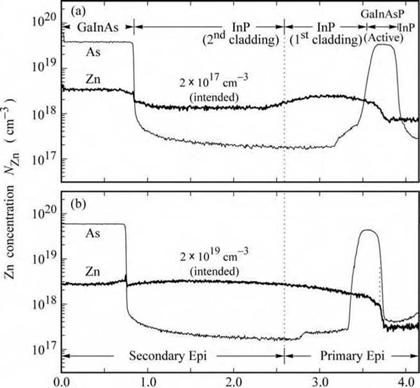
Fig. 7.5. Secondary ion mass spectrometry (SIMS) profile of Zn in a GalnAsP/InP double heterostructure. The structure uses Zn as a p-type dopant. Part (a) shows no p-n junction displacement. Part (b) shows p-n junction displacement caused by high Zn doping of the upper cladding region (after Schubert et al., 1995). |
|
Depth z (pm) |
An example of a Zn acceptor profile in a GaInAsP/InP double heterostructure measured by secondary ion mass spectrometry (SIMS) is shown in Fig. 7.5. In Fig. 7.5 (a), the top confinement layer has a moderate intended doping concentration of 2 x 1017 cm-3. The Zn profile indicates that the Zn is mostly confined to the upper confinement layer, even though some Zn has evidently diffused into the active region. In Fig. 7.5 (b), however, the top confinement layer has a high intended doping concentration of 2 x 1019 cm-3. The profile indicates that Zn has strongly diffused into the active region. The p-n junction is displaced to the edge of the active region. As a result, the device shown in Fig. 7.5 (b) has a much lower quantum efficiency than the device shown in Fig. 7.5 (a).
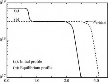
A model explaining the p-n junction displacement in the GalnAsP/InP DH structure is illustrated in Fig. 7.6 (Schubert et al., 1995). It is assumed in this model that the Zn diffusion coefficient increases rapidly above a critical concentration Arcritical. If this concentration is exceeded during growth, Zn will redistribute until the concentration falls below the critical concentration. As a result, Zn can diffuse into and through the active region of the double heterostructure. It is remarkable that the p-n junction displacement can occur, even if the intended Zn concentration in the confinement region in the vicinity of the active region is quite low.
|
|
|
Depth z (arbitrary units) |
|
Fig. 7.6. P-n junction displacement process caused by excessive doping of the cladding region. If the acceptor dopant has a highly concentration-dependent diffusion constant and the diffusion constant increases strongly above a critical concentration, ^critical’ P-" iunction displacement occurs in the active region (after Schubert et al., 1995). |


 Опубликовано в