Non-radiative recombination
 18 марта, 2014
  admin
admin It is imperative that the material comprising the active region of light-emitting devices is of very high crystal quality. Deep levels caused by point defects, unwanted impurities, dislocations, and other defects must have a very low concentration.
Similarly, surface recombination must be kept at the lowest possible levels. This can be accomplished by keeping free surfaces several diffusion lengths away from regions in which both electrons and holes reside, i. e. any surfaces must be “out of reach” of the active region.
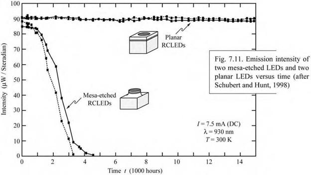
Mesa-etched LEDs and lasers, in which the mesa etch exposes the active region to air, generally have low internal efficiencies due to surface recombination. Surface recombination also leads to a reduction of the lifetime of LEDs. Surface recombination generates heat at the semiconductor surface, which can lead to structural defects such as dark-line defects that further reduce the efficiency of LEDs.
Figure 7.11 shows the light intensity of two mesa-etched and two planar LEDs versus time. Inspection of Fig. 7.11 reveals that (/) the light intensity at t = 0 h of the mesa-etched LEDs is slightly lower than that of the planar structure and that (ii) the lifetime of the mesa-etched device is much shorter. In the planar device, electron-hole recombination occurs below the top metal contact far away from the sidewall surfaces of the device. Thus, no intensity reduction or degradation mediated by surface recombination is expected for the planar device.
|
|
Note that the presence of surfaces does not reduce the radiative efficiency if only one type of carrier is present, e. g. near the top contact of the device. Surfaces in such unipolar regions do not have any deleterious effects.
|
|
7.6 Lattice matching
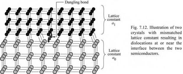
In double heterostructures, the active region material is different from the confinement layer material. However, both materials should have the same crystal structure and lattice constant. If the semiconductors do not have the same lattice constant, defects will occur at or near the
interface between the two semiconductors. Figure 7.12 illustrates that dangling bonds can result as a consequence of mismatched semiconductors.
|
|
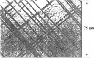
Inspection of Fig. 7.12 reveals that a row of dangling bonds can occur at the interface of two mismatched materials. Such misfit dislocation lines are straight lines of extended defects that can be made visible by cathodo-luminescence. Usually a cross-hatched pattern can be observed in the micrograph of mismatched structures. The effect of misfit dislocation lines on radiative recombination is shown in Fig. 7.13. The cathodo-luminescence micrograph shown in Fig. 7.13 exhibits a cross-hatch pattern of dark lines. The lines appear darker than the surrounding areas since carriers recombine non-radiatively at these dislocation lines.
Fig. 7.13. Cathodo-luminescence image of a 0.35 |im thick Ga0.95ln0.05As layer grown on a GaAs substrate. The dark lines forming a cross-hatch pattern are due to misfit dislocations (after Fitzgerald et al., 1989).
|
(b) |
|
(a) |
|
О О |
|
о о |
|
о о |
|
о о |
|
о о |
|
о—о о—о • -*-• ап t •—• |
|
о О О |
|
о о |
|
о о |
|
о о |
|
о о |
|
о—о о—о |
|
0- |
K Oi |
"0 - H ° |
|
0- |
-oJ |
°0 —0 |
|
0- |
-0- |
-0 |
|
KeiH 'I |
|
In-plane lattice constant Normal lattice constant a„ |
|
Lattice constant °0 |
|
Lattice constant |
Fig. 7.14. (a) Cubic-symmetry crystals with equilibrium lattice constant aj and Oq.
(b) Thin, coherently strained layer with equilibrium lattice constant aj sandwiched between two semiconductors with equilibrium lattice constant aq. The coherently strained layer assumes an in-plane lattice constant an and a normal lattice constant a.
Misfit dislocations may not occur directly at the interface between the mismatched materials but may start to form near the interface. This is because the mismatched crystal grown on top of the semiconductor will initially be strained elastically and assume the same in-plane lattice constant as the underlying substrate. This situation is shown in Fig. 7.14, where a thin layer is strained so that it has the same in-plane lattice constant as the underlying material. Once the energy needed to strain the lattice exceeds the energy required to form misfit dislocations, the thin film relaxes to its equilibrium lattice constant by forming misfit dislocations. The layer thickness at which misfit dislocations are formed is called the critical thickness. It has been calculated by Matthews and Blakeslee (1976). If the layer is thinner than the critical thickness given by the Matthews-Blakeslee law, a thin dislocation-free layer can be grown even if the layers have different lattice constants.
|
|
|
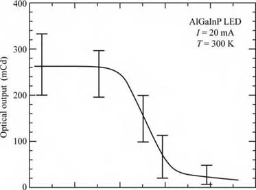
Fig. 7.15. Optical output intensity of an AlGaInP LED driven with an injection current of 20 mA versus the lattice mismatch between the AlInGaP active region and the GaAs substrate (after Watanabe and Usui, 1987). |
|
0 2x10 4x10 6x10 8x10 10xl0_3 Lattice mismatch Дa/a |
The density of misfit dislocation lines per unit length is proportional to the lattice mismatch. Consequently, the efficiency of LEDs is expected to drop as the lattice mismatch is increased. Figure 7.15 shows the decrease of the optical intensity of an AlGaInP LED grown on a GaAs substrate. The AlGaInP material used for high-brightness red LEDs is matched to the GaAs substrate. Figure 7.15 reveals that the light output drops strongly as the mismatch, defined as Aa / a, exceeds 3 x 10⁻³.
Red GaAsP LEDs are grown on GaAs substrates and the active layers are mismatched to the substrate. As a result, red GaAsP LEDs are low cost but also low efficiency. The homojunction
GaAsP LEDs grown on GaAs substrates are the lowest-cost red devices available.
Whereas the III-V arsenide and III-V phosphide material family is strongly affected by surface recombination and lattice mismatch, the III-V nitride material family is less so. One of the reasons for the insensitivity of the GaN material family to dislocation defects is the lower electrical activity that dislocations in these materials appear to exhibit. Another reason is the smaller diffusion length of carriers in the GaN material family. If the mean distance between dislocations is larger than the diffusion length, in particular the hole diffusion length, non - radiative recombination at these dislocations will not be severe. Another model explaining the high efficiency of GaInN is based on compositional fluctuations of the ternary alloy, which localize carriers preventing them from diffusing towards dislocation lines.


 Опубликовано в