LED basics: Electrical properties
 6 марта, 2014
  admin
admin 2.1 Diode current—voltage characteristic The electrical characteristics of p-n junctions will be summarized, however, a detailed derivation of the results will not be provided in this chapter. We consider an abrupt p-n junction with a donor concentration of ND and an acceptor concentration of NA. All dopants are assumed to be fully ionized so that the free electron concentration is given by n = ND and the free hole concentration is given by p = NA. It is further assumed that no compensation of the dopants occurs by unintentional impurities and defects.
In the vicinity of an unbiased p-n junction, electrons originating from donors on the n-type side diffuse over to the p-type side where they encounter many holes with which they recombine. A corresponding process occurs with holes that diffuse to the n-type side. As a result, a region near the p-n junction is depleted of free carriers. This region is known as the depletion region.
|
|
|
(a) p-n junction under zero bias |
|
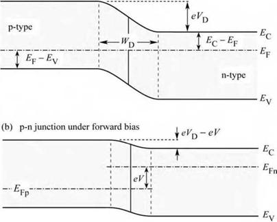
Fig. 4.1. P-n junction under (a) zero bias and (b) forward bias. Under forward-bias conditions, minority carriers diffuse into the neutral regions where they recombine. |
In the absence of free carriers in the depletion region, the only charge in the depletion region is from ionized donors and acceptors. These dopants form a space charge region, i. e. donors on the n-type side and acceptors on the p-type side. The space charge region produces a potential that is called the diffusion voltage, VD. The diffusion voltage is given by
|
(4.1) |
|
Vd = |
|
e |
|
kL ln NA ND |
|
n |
where Na and ND are the acceptor and donor concentrations, respectively, and ni is the intrinsic carrier concentration of the semiconductor. The diffusion voltage is shown in the band diagram of Fig. 4.1. The diffusion voltage represents the barrier that free carriers must overcome in order to reach the neutral region of opposite conductivity type.
The width of the depletion region, the charge in the depletion region, and the diffusion voltage are related by the Poisson equation. It is therefore possible to determine the depletion layer width from the diffusion voltage. The depletion layer width is given by
|
2 є |
|
(Vd - V) |
|
(4.2) |
|
Wd = |
|
II |
|
N |
|
e |
|
D J |
|
1 1 • + ■ |
|
NA |
where є = sr є0 is the dielectric permittivity of the semiconductor and V is the diode bias voltage.
Upon application of the bias voltage to the p-n junction, the voltage is going to drop across the depletion region. This region is highly resistive due to the fact that it is depleted of free carriers. An external bias therefore decreases or increases the p-n junction barrier for forward or reverse bias, respectively. Under forward-bias conditions, electrons and holes are injected into the region with opposite conductivity type and current flow increases. The carriers diffuse into the regions of opposite conductivity type where they will eventually recombine, thereby emitting a photon.
|
|
The current-voltage (I-V) characteristic of a p-n junction was first developed by Shockley and the equation describing the I-V curve of a p-n junction diode is therefore referred to as the Shockley equation. The Shockley equation for a diode with cross-sectional area A is given by
(4.3)
where Dnp and Tnp are the electron and hole diffusion constants and the electron and hole
|
4.1 Diode current-voltage characteristic |
|
minority-carrier lifetimes, respectively. Under reverse-bias conditions, the diode current saturates and the saturation current is given by the factor preceding the exponential function in the Shockley equation. The diode I-V characteristic can be written as |
|
(?eVkT - 1) |
|
D |
|
p ni |
|
n ni |
|
I = Isle |
|
with |
|
Is = eA |
|
(4.4) |
|
+ |
|
Tp nd |
|
Tn NA |
|
Under typical forward-bias conditions, the diode voltage is V>> kT / e, and thus [exp (eV/ kT) - 1] * exp (eV/ kT). Using Eq. (4.1), the Shockley equation can be rewritten, for forward-bias conditions, as |
|
Л |
|
Dp |
|
D |
|
ee (V - VdV kT |
|
nN |
|
(4.5) |
|
I = eA |
|
na + |
|
D |
|
V |
|
T |
|
p |
|
n |
|
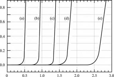
The exponent of the exponential function in Eq. (4.5) illustrates that the current strongly increases as the diode voltage approaches the diffusion voltage, i. e. V* VD. The voltage at which the current strongly increases is called the threshold voltage and this voltage is given by Vth * Vd. The band diagram of a p-n junction, shown in Fig. 4.1, also illustrates the separation of the Fermi level from the conduction and valence band edge. The difference in energy between the Fermi level and the band edges can be inferred from Boltzmann statistics and is given by |
|
n |
|
Eq - Ef = - kT ln |
|
for the n-type side |
|
(4.6) |
|
-F |
|
Nc |
|
and |
|
Ef - Ev = - kT ln |
|
for the p-type side. |
|
(4.7) |
|
Nv |
|
The band diagram shown in Fig. 4.1 illustrates that the following sum of energies is zero: |
|
eVD - Eg + (EF - EV) + (EC - EF) = 0 . |
|
(4.8) |
|
In highly doped semiconductors, the separation between the band edges and the Fermi level is small compared with the bandgap energy, i. e. (Ec - Ef) << Eg on the n-type side and (Ef - |
EV) << Eg on the p-type side. Furthermore, these quantities depend only weakly (logarithmic dependence) on the doping concentration as inferred from Eqs. (4.6) and (4.7). Thus, the third and fourth summand of Eq. (4.8) can be neglected and the diffusion voltage can be approximated by the bandgap energy divided by the elementary charge
Vth - Vd - Eg/г . (4.9)
|
|
|
Diode voltage V (V) |
|
Fig. 4.2. Room-temperature current-voltage characteristics of p-n junctions made from different semiconductors. |
|
T= |
295 К |
|
|
(a) |
Ge |
£g « 0.7 eV |
|
(b) |
Si |
fg - 1.1 eV |
|
(c) |
GaAs |
Eg = 1.4 eV |
|
(d) |
GaAsP |
Eg » 2.0 eV |
|
(e) |
GaInN |
Eg = 2.9 eV |
|
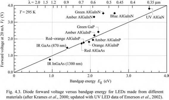
The forward diode voltage at a diode current of 20 mA versus bandgap energy for LEDs emitting in the ultraviolet, visible, and infrared wavelength range is shown in Fig. 4.3 (Krames et al., 2000; Emerson et al., 2002). The solid line illustrates the expected forward diode voltage. The line equals the bandgap energy divided by the elementary charge. Inspection of the figure reveals that most semiconductor LEDs follow the solid line, except for LEDs based on III-V nitrides. This peculiarity is due to several reasons. Firstly, large bandgap discontinuities occur in the nitride material system, which cause an additional voltage drop. Secondly, the contact technology is less mature in the nitride material system, which causes an additional voltage drop at the ohmic contacts. Thirdly, the p-type conductivity in bulk GaN is generally low. Lastly, a parasitic voltage drop can occur in the n-type buffer layer. |
Several diode I-V characteristics of semiconductors made from different materials are shown in Fig. 4.2 along with the bandgap energy of these materials. The experimental threshold voltages shown in the figure, and the comparison with the bandgap energy of these materials, indicates that the energy gap and the threshold voltage indeed agree reasonably well.
|
|
Assuming a chip area of 250 |jm x 250 ^m and a current of 20 mA, the current density used in Fig. 4.3 to characterize the forward voltage is 32 A/cm2. Typical current densities in LEDs range from 30 A/cm2 in low-power devices to 100 A/cm2 in high-power devices.


 Опубликовано в