Double heterostructures
 17 марта, 2014
  admin
admin The lifetimes derived from the bimolecular rate equation show that the radiative rate increases with the free-carrier concentration for both the low excitation limit as well as the high excitation limit. It is therefore important that the region in which recombination occurs has a high carrier concentration. Double heterostructures are an excellent way to achieve such high carrier concentrations.
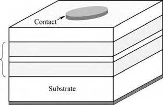
A double heterostructure (DH) consists of the active region in which recombination occurs and two confinement layers cladding the active region. A double heterostructure LED structure is shown schematically in Fig. 7.1. The two cladding or confinement layers have a larger bandgap than the active region. If the bandgap difference between the active and the confinement regions is AEg, then the band discontinuities occurring in the conduction and valence bands follow the relation
|
(7.1) |
|
Eg |
|
- Eg |
|
V |
|
cladding |
|
active |
|
= AEg = AEc + AE |
Both band discontinuities, AEC and AEV, should be much larger than kT in order to avoid carrier escape from the active region into the confinement regions.
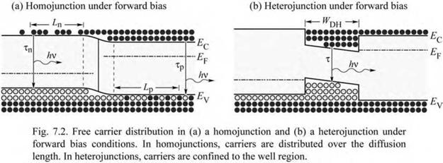
The effect of a double heterostructure on the carrier concentration is illustrated schematically in Fig. 7.2. In the case of a homojunction, carriers diffuse to the adjoining side of the junction
under forward bias conditions. Minority carriers are distributed over the electron and hole diffusion lengths as illustrated in Fig. 7.2 (a). In III-V semiconductors, diffusion lengths can be 10 |im or even longer.
|
|
|
Current spreading layer Top confinement layer Active region Bottom confinement layer Substrate Contact |
|
Fig. 7.1. Illustration of a double heterostructure consisting of a bulk or quantum well active region and two confinement layers. The confinement layers are frequently called cladding layers. |
|
Double |
|
(DH) |
|
|
The wide distribution of carriers and the correspondingly low carrier concentration (particularly towards the end of the diffusion tail) can be avoided by the employment of double heterostructures. Carriers are confined to the active region, as shown in Fig. 7.2 (b), as long as the barrier heights are much higher than the thermal energy kT. Today virtually all high - efficiency LEDs use double heterostructure designs.
Double heterostructures are used for bulk as well as quantum well active regions. Quantum
well active regions provide additional carrier confinement to the narrow well regions, which can further improve the internal quantum efficiency. On the other hand, if a quantum well active region is used, the barriers between the wells will impede the flow of carriers between adjacent wells. Thus the barriers in a multi-quantum well active region need to be sufficiently “transparent” (low and/or thin barriers) in order to allow for efficient carrier transport between the wells and to avoid the inhomogeneous distribution of carriers within the active region.
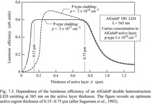
The thickness of the active region in a DH has a strong influence on the internal quantum efficiency of an LED. Typical active region thicknesses are a few tenths of a micrometer for bulk active regions and even thinner for quantum well active regions. The dependence of device efficiency on the active region thickness is shown in Fig. 7.3 (Sugawara et al., 1992). Inspection of the figure shows that the optimum thickness for an AlGaInP active region is between 0.15 and 0.75 |im.
|
|
If the active region in a double heterostructure becomes too thick, e. g. larger than the diffusion length of carriers, the advantage of the double heterostructure is lost and carriers are distributed as they are in homojunctions. On the other hand, if the active region of a double heterostructure becomes too thin, the active region tends to overflow at high injection current levels.
Doping of the active region and confinement layers plays a crucial role in the efficiency of double heterostructure (DH) LEDs. The influence of the doping on the internal efficiency is multifaceted. Firstly, we consider the doping of the active region.
The active region of III-V arsenide and phosphide DH LEDs must not be heavily doped. Heavy doping with either p-type or n-type dopants would place the p-n junction effectively at the edge of the DH well region, i. e. at the active/confinement interface, thereby promoting carrier spill-over into one of the confinement regions. Diffusion of carriers into the cladding region decreases the radiative efficiency. Thus heavy doping of the active region is rarely done in III-V arsenide and phosphide DH LEDs.
Therefore it is required that the active region is either doped at a level lower than the doping concentration in the confinement regions or left undoped. Typically the doping concentration in intentionally doped active regions is either p-type or n-type in the 1016 to low 1017 cm-3 range. Frequently the active layer is left undoped.
|
|
|
n-type active ] p-type active layer J layer |
|
AlGaInP DH LED |
|
о |
|
0.0 |
|
2.0 1.0 0.0 и-type (x 1017 cm-3) |
|
1.0 2.0 3.0 /Муре ( x 10і7 cm-3) |
P-type doping of the active region is more common than n-type doping of the active region, due to the generally longer electron-minority-carrier diffusion length compared with the hole- minority-carrier diffusion length. (Note that electrons generally have a higher mobility than holes in III-V semiconductors.) Thus, p-type doping of the active region ensures a more uniform carrier distribution throughout the active region.
Fig. 7.4. Dependence of the luminous efficiency of an AlGaInP double heterostructure LED emitting at 565 nm on the active layer doping concentration (after Sugawara et al., 1992).
Carrier concentration in active layer
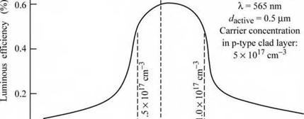
The dependence of device efficiency on the doping concentration of the active region in an AlGaInP DH LED is shown in Fig. 7.4 (Sugawara et al., 1992). Inspection of the figure shows that a high quantum efficiency is obtained only for n-type doping concentrations below 5 x 1016 cm-3, and below 1 x 1017 cm-3 for p-type active layers.
Figure 7.4 also reveals that light p-type doping of the active region is preferable over light n-
type doping. Therefore, most active layers of LEDs and lasers are lightly doped with acceptors. Electrons with their larger diffusion length are also more likely to diffuse into the p-type confinement layer if the active region is doped n-type.
Intentional doping of the active region can have advantages as well as disadvantages. The carrier lifetime depends on the concentration of majority carriers. In the low-excitation regime, the radiative carrier lifetime decreases with increasing free carrier concentration, i. e. doping concentration. As a result, the radiative efficiency increases. An example of a material whose luminescence efficiency increases with doping concentration is Be-doped GaAs. It is well known that the radiative efficiency of Be-doped GaAs increases with the Be doping level in the moderate doping concentration range.
On the other hand, dopants may, especially at high concentrations, introduce defects that act as recombination centers. High concentrations of intentional dopants lead to an increased concentration of native defects due to the dependence of the native and non-native defect concentrations on the Fermi level (see, for example, Longini and Greene, 1956; Baraff and Schluter, 1985; Walukiewicz, 1988, 1989, 1994; Neugebauer and Van de Walle, 1999).
The epitaxial growth process may also depend on doping. Doping atoms can act as
surfactants, i. e. surface-active reagents. For example, a surfactant can increase the surface
diffusion coefficient, thereby improving crystal quality. There are many other ways by which surfactants influence the growth process. These processes are generally not understood in great detail. However, the improvement of crystal quality has been found in a number of cases. During the growth of InGaN, for example, a marked improvement of crystal quality has been found upon doping with silicon (Nakamura et al., 1996, 1998). The quantum barriers in III-V nitride multiple-quantum well structures are in fact often doped with silicon at a high level, e. g. 2 x 1018 cm-3. The increase in device efficiency found for high doping may be due to the screening of internal polarization fields which reduces the overall potential drop within the active region.


 Опубликовано в