Double heterostructures
 21 марта, 2014
  admin
admin Virtually all LED structures employ double heterostructures. They consist of two confinement layers and the active region. The band diagram of a double heterostructure is shown in Fig. 9.2. The active region has a smaller bandgap energy than the two confinement regions. As a result, the confinement regions are transparent to the light emitted by the active region. Since the confinement regions are relatively thin, they can be considered, for all practical purposes, to be totally transparent.
|
"V |
|
Fig. 9.2. Double hetero-structure with optically transparent confinement regions. Reabsorption in the active region is unlikely due to the high carrier concentration in the active region and the resulting Burstein-Moss shift of the absorption edge. |
|
Transparent Light-emitting Transparent confinement region active region confinement region
|
|
Note, however, that the active region is in equilibrium sufficiently far away from the current - injected region. These regions are not current injected and thus will absorb near-bandgap light emitted by the active region. To reduce optical losses by absorption, the active region should have a high internal quantum efficiency to make re-emission of absorbed photons likely. |
Reabsorption of light by the active region in the current-injected area below the top contact can also be neglected. The active region is, under normal injection conditions, injected with high current densities so that the electron and hole quasi-Fermi levels rise into the bands, as illustrated in Fig. 9.2. As a result, the active region is practically transparent for near-bandgap emission under high injection conditions.
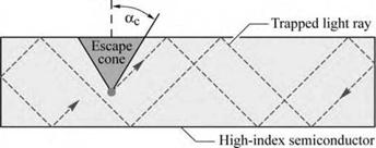
9.1 Shaping of LED dies One of the most important problems facing high-efficiency LEDs is the occurrence of trapped light within a high-index semiconductor. The occurrence of trapped light is illustrated in Fig. 9.3. A light ray emitted by the active region will be subject to total internal reflection, as predicted by Snell’s law. In the high-index approximation, the angle of total internal reflection is given by
ac = V1 (9.9)
|
|
where ns is the semiconductor refractive index and the critical angle ac is given in radians. For high-index semiconductors, the critical angle is quite small. For example, for a refractive index of 3.3, the critical angle for total internal reflection is only 17°. Thus most of the light emitted by the active region is trapped inside the semiconductor. The trapped light is most likely to be absorbed by the thick substrate. Once absorbed, the electron-hole pair is likely to recombine non-radiatively due to the comparatively low quality and efficiency of the substrate.
Fig. 9.3. “Trapped light” in a rectangular-parallelepiped-shaped semiconductor unable to escape for emission angles greater than ac due to total internal reflection.
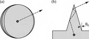
The light-escape problem has been known since the infancy of LED technology in the 1960s. It has also been known that the geometrical shape of the LED die plays a critical role. The optimum LED would be spherical in shape with a point-like light-emitting region in the center of the LED. Such a spherical LED is shown in Fig. 9.4 (a). Light emanating from the point-like active region is incident at a normal angle at the semiconductor-air interface. As a result, total internal reflection does not occur in such LEDs. Note, however, that the light is still subject to Fresnel reflection at the interface unless the sphere is coated with an anti-reflection coating.
LEDs with a hemispherical dome-like structure (Carr and Pittman, 1963) as well as other shapes, e. g. inverted, truncated cones (Franklin and Newman, 1964; Loebner, 1973) have been demonstrated to improve extraction efficiency over conventional designs, i. e. rectangular parallelepiped chips. However, the practical utility of such devices has not been realized primarily due to the high cost associated with shaping of individual LED dies.
Fig. 9.4. Schematic illustration of different geometric shapes for LEDs with perfect extraction efficiency, (a) Spherical LED with a point-like light-emitting region at the center of the sphere, (b) A cone-shaped LED.
|
|
Unfortunately, spherical LEDs with a point-like light source in the center of the LED are somewhat impractical devices. Semiconductor fabrication technology is, in view of the flat substrates used in epitaxial growth, a planar technology. Thus spherical LEDs are difficult to fabricate using conventional planar technology.
Another interesting LED structure is a cone-shaped structure, as shown schematically in Fig. 9.4 (b). Light rays are emanating from the active region at or below the base of the cone. The light rays incident at the cone-air boundary are either transmitted through the semiconductor-air interface or guided by the cone. The guided rays undergo multiple reflections. As light rays undergo multiple reflections, they will form a progressively increasing angle of incidence at the semiconductor-air interface. As a result, light guided by the cone will eventually have nearnormal incidence and escape from the cone. Although an interesting concept, cone-shaped LEDs are difficult to fabricate and manufacture.
The most common LED structure has the shape of a rectangular parallelepiped as shown in Fig. 9.5 (a). Such LED dies are fabricated by cleaving the wafer along its natural cleavage planes. The LEDs have a total of six escape cones, two of them perpendicular to the wafer surface, and four of them parallel to the wafer surface. The bottom escape cone will be absorbed by the substrate if the substrate has a lower bandgap than the active region. The four in-plane escape cones will be at least partially absorbed by the substrate. Light in the top escape cone will be obstructed by the top contact, unless a thick current-spreading layer is employed. Thus the simple rectangular parallelepiped LED is clearly a structure with low extraction efficiency. However, a substantial advantage of such LEDs is the low manufacturing cost.
An LED with a cylindrical shape is shown in Fig. 9.5 (b). The cylindrical LED has the advantage of higher extraction efficiency compared with a cube-shaped LED. An escape ring, as shown in Fig. 9.5 (b), replaces the four in-plane escape cones of the rectangular LED, which results in a substantial improvement of the extraction efficiency. Cylindrical-shaped LEDs require one more processing step (etching step) compared with rectangularly shaped LEDs.
|
Fig. 9.5. Illustration of different geometric shapes of LEDs, (a) Rectangular parallelepipedal LED die with a total of six escape cones, (b) Cylindrical LED die with a top escape cone and a side escape ring. |
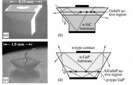
Commercially available die-shaped devices include pedestal-shaped GalnN/SiC LEDs with trade name “Aton” (Osram, 2001) and truncated inverted pyramid (TIP) AlGaInP/GaP LEDs (Krames et al., 1999). Photographs and schematic structures of the two devices are shown in Fig. 9.6. Ray traces indicated in the figure show that light rays entering the base of the pyramids escape from the semiconductor after undergoing one or multiple internal reflections. The pedestal and TIP geometries reduce the mean photon path length within the die, and thus reduce internal absorption losses. The increase in efficiency of pedestal-shaped devices is about a factor of 2 compared to rectangular-parallelepiped-shaped devices (Osram, 2001).
|
|
|
p-type contact |
|
Fig. 9.6. Die-shaped devices: (a) Blue GaInN emitter on SiC substrate with trade name “Aton”. (b) Schematic ray traces illustrating enhanced light extraction, (c) Micrograph of truncated inverted pyramid (TIP) AlGaInP/GaP LED. (d) Schematic diagram illustrating enhanced extraction (after Osram, 2001; Krames etal., 1999). |
The geometric shape of the LED, in particular the side-wall angle, is chosen in such a way that trapping of light is minimized. Ray tracing computer models are employed to maximize the escape probability from the semiconductor. The optimum angle of the TIP sidewall tilt is 35 °
(Krames et al., 1999). The TIP LED is a high-power LED with a large p-n junction area of 500 ^m x 500 ^m. The luminous source efficiency of TIP LEDs exceeds 100 lm/W and is one of the highest ever achieved with LEDs.
The TIP LED performance versus injection current is shown in Fig. 9.7 (Krames et al.,
1999) . A peak luminous efficiency of 102 lm/W was measured for orange-spectrum (X « 610 nm) devices at an injection current of 100 mA. This luminous efficiency exceeds that of most fluorescent (50-100 lm/W) and all metal-halide (68-95 lm/W) lamps. In the amber color regime, the TIP LED provides a photometric efficiency of 68 lm/W (X « 598 nm). This efficiency is comparable to the source efficiency of 50 W high-pressure sodium discharge lamps. A peak external quantum efficiency of 55% was measured for red-emitting (X « 650 nm) TIP LEDs. Under pulsed operation (1% duty cycle), an efficiency of 60.9% was achieved (data not shown), which sets a lower bound on the extraction efficiency of these devices.
60
|
50 |
|
" TIP LED |
|
0) С |
|
С 40 |
|
— u £ V £ С В |
|
зо |
|
LJ LED |
|
20 10 |
|
с о |
|
1000 |
|
AlGalnP/GaP red LED X = 650 nm T = 300 к Aj = 0.25 mnr |
|
10 100 DC forward current I (mA) |
|
-1.4 |
|
_L |
|
Fig. 9.7. External efficiency vs. forward current for red-emitting (650 nm) truncated inverted pyramid (TIP) LEDs and large junction (LJ) LEDs mounted in power-lamp packages. The TIP LED exhibits a 1.4 times improvement in extraction efficiency compared with the LJ device, resulting in a peak external quantum efficiency of 55% at 100 mA (after Krames et al., 1999). |
The rectangular parallelepiped and cylindrical LED structures can be fabricated with wafer- scale processing steps. Advanced structures, such as the TIP LED, are also fabricated by wafer - scale processes, namely a sawing process employing a beveled dicing blade (Haitz, 1992). The manufacturing cost of LEDs requiring die-level processing steps is much higher compared with LEDs manufactured with wafer-scale processes.
The use of tapered output couplers in LEDs has been reported by Schmid et al. (2000, 2001, 2002). For GaAs-based infrared devices, external quantum efficiencies near 50% have been demonstrated with devices having a tapered output coupler. However, due to the area requirements of the output coupler, the current-injected region of the device is much smaller than the overall device area and thus the total emission power is quite small.
9.2 Textured semiconductor surfaces Other ways to increase the light extraction efficiency in GaAs-based devices include the use of roughened or textured semiconductor surfaces (see, for example, Schnitzer et al., 1993; Windisch et al., 1999, 2000, 2001, 2002). External quantum efficiencies near 50% have been reported for GaAs-based surface-textured devices. A detailed discussion of properties and fabrication of microstructured surfaces was given by Sinzinger and Jahns (1999).
After initial positive reports on enhancement of light extraction in devices having textured surfaces, the optimism of the technical community was dampened when it became clear that much of the increase in light extraction was lost during the polymer encapsulation process of the semiconductor chip. That is, although a strong increase of light extraction had been found in unpackaged chip measurements the gain practically vanished after chip encapsulation.
|
|
|
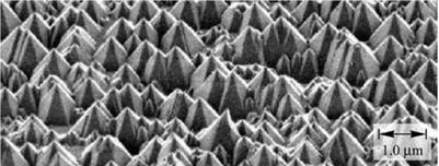
Fig. 9.8. Scanning electron micrograph of strongly textured GaN surface (after Haerle, 2004). |
There are several recent reports on the increase of light extraction in GaN-based devices with substantial surface texture achieved by wet chemical etching. For many years, it had been assumed that GaN with Ga-polarity cannot be etched by any wet chemical etch. However, Stocker et al. (1998a) showed that, although the c-plane of GaN lacks etchability, the a - and m - planes of GaN can be etched by a number of wet chemical etches including hot KOH and H3PO4. Stocker et al. (1998b, 2000) also showed that these etches are crystallographic in nature, which allows one to create pyramid-like structures and atomically smooth surfaces suited for laser fabrication. Wet chemical etching and photoelectrochemical etching can be used to create a substantial amount of surface roughness on GaN. An example of a very rough GaN surface is shown in Fig. 9.8 (Haerle, 2004).
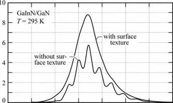
The increase in light extraction from a surface-textured GaInN device (with the device having the strongly textured surface shown in Fig. 9.8) is shown in Fig. 9.9 (Haerle, 2004). The author estimated the increase in output power to be 40-50%. Similar results were reported independently by Gao et al. (2004) and Fujii et al. (2004). Note that the interference fringes,
observed for the GaN device having the smooth surface, completely vanish for the surface- textured film. The interference fringes are caused by the Fabry-Perot cavity formed by the GaN-air interface and the sapphire-GaN interface which form the two reflectors of the cavity (Billeb et al, 1997).
|
|
|
Fig. 9.9. Emission spectrum of GaInN blue LED with and without surface texture. The spectrum exhibits Fabry-Perot interference fringes for the device with a smooth surface (after Haerle, 2004). |
|
400 420 440 460 480 500 520 540 |
|
Wavelength X (nm) |
|
|
///, • » ~v7bVb~'
Fig. 9.10. Schematic illustration of waveguide with (a) no surface texture, (b) weak surface texture, and
(c) strong surface texture, resulting in specular reflection, mixed reflection and scattering, and strong scattering, respectively.
The transition from a smooth surface to a strongly textured surface and the implication on ray propagation is shown in Fig. 9.10. A perfectly smooth surface, i. e. a specular surface, results in waveguided modes that cannot escape, as shown in Fig. 9.10 (a). For a strongly scattering surface, i. e. a lambertian or diffuse surface, only one or a few scattering events are sufficient to out-couple the light as shown in Fig. 9.10 (c). The intermediate case is shown in Fig. 9.10 (b). Because the light-out-coupling efficiency depends on the degree of diffusivity, it would be desirable to quantify the degree of surface diffusivity (for a discussion of the quantification of the diffuseness of a surface, see the chapter entitled “Reflectors” in this book).
The optical microscopic inspection of chip surfaces of GaInN high-performance devices (Nichia, 2005) reveals that the chip surface is textured and appears as white, which is a clear indication that the surface was strongly textured to create a diffuse, strongly scattering surface.



 Опубликовано в