AlGaInP/GaAs RCLEDs emitting at 650 nm
 7 апреля, 2014
  admin
admin RCLEDs have also been demonstrated in the visible wavelength range using the AlGaInP material system (Streubel et al., 1998; Whitaker, 1999; Wirth et al., 2001, 2002). The AlGaInP material system is commonly used for high-brightness red, orange, and yellow emitters and can be grown lattice matched on GaAs substrates. The active region of RCLEDs is an AlGaInP/GaInP multiple-quantum well structure emitting at 650 nm. The RCLEDs are suited for
use in communication systems using plastic optical fibers. It is difficult to fabricate VCSELs in this wavelength range due to the unavailability of lattice-matched and transparent DBR materials with a large refractive-index contrast.
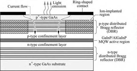
The basic structure of a top-emitting AlGaInP RCLED emitting at 650 nm is shown in Fig. 15.9. The device consists of an AlGaInP/GaInP MQW active region and AlGaInP cladding layers. The DBRs consist of AlAs/AlGaAs layers. The Al content in the AlGaAs layers of the DBR is chosen to be sufficiently high to make the DBR transparent to the light emitted by the active region. As a result, the index contrast of the AlAs/AlGaAs DBR layers is somewhat low.
|
|
|
Fig. 15.9. Structure of a GalnP/AlGalnP/GaAs MQW RCLED emitting at 650 nm used for plastic optical fiber applications (after Whitaker, 1999) |
|
|
The RCLED has a ring-shaped top contact configuration. The current is funneled into the center region of the ring using ion implantation to create an insulating region under the ringshaped metalization. Hydrogen and, more frequently, oxygen implantation is used to render the semiconductor highly resistive. Note that the ion-implanted region is located in the p-type region
only and does not extend into the active region, thereby avoiding the creation of defects in the active region where they would act as luminescence killers.
Packaged RCLEDs in a lensed TO package and in a pig-tailed package are shown in Figs. 15.10 (a) and (b) (Mitel Corporation, 1999), respectively. The lens is used for beam collimation, thereby enhancing the coupling efficiency to fibers.
|
|
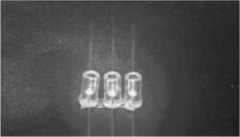
Three RCLEDs under current injection conditions are shown in Fig. 15.11 (Osram Opto Semiconductors Corporation). The picture shows that the emission pattern is directed towards the surface normal of the devices. The emission wavelength is 650 nm.
Fig. 15.11. AlGaInP/GaAs RCLEDs emitting at 650 nm. Note the forward-directed emission pattern similar to that of a semiconductor laser (courtesy of Osram Opto Semiconductors Corporation, Germany, 1999).
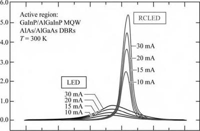
Optical spectra of a 650 nm RCLED and of a conventional LED injected at different current levels are shown in Fig. 15.12. The spectra are measured after the light is coupled into a plastic optical fiber. Thus, the magnitude of the spectra is a direct measure of the device efficiency and of the coupling efficiency. Inspection of the figure reveals several features. Firstly, the RCLED has a higher coupled peak power as well as integrated power than the LED. Secondly, the RCLED has a higher spectral purity than the LED.
Streubel et al. (1998) also reported that the emission spectrum was, at room temperature, intentionally blue-shifted with respect to the cavity resonance in order to improve the temperature stability of the RCLED output power. This cavity tuning results in a heart-shaped (double-lobed) emission pattern at room temperature, because the resonance wavelength of the cavity decreases for off-normal emission directions. As the temperature increases, the natural emission spectrum from the active region red-shifts, so that the cavity resonance (along the normal direction) has a better overlap with the natural emission spectrum. As a result, the temperature sensitivity of the RCLED is reduced. The natural emission spectrum red-shifts at a rate of about 0.5 nm/°C, whereas the cavity resonance shifts at only about one-tenth of that rate.
|
|
|
*o 3 Л - O Си 3 N |
|
Р 3 = р |
|
•j с. ZJ Ш с- |
|
600 620 640 660 Wavelength X (nm) |
|
680 |
|
700 |
|
Fig. 15.12. Spectra of light coupled into a plastic optical fiber from a GalnP/AlGalnP MQW RCLED and a conventional GalnP/AlGalnP LED at different drive currents. Note the narrower spectrum and higher coupled power of the RCLED (after Streubel etal, 1998). |
|
*§ СЛ E C - Г- 1) С о ■- л u б С к О "О о о в а |
15.4 Large-area photon recycling LEDs
Instead of devising ways to reduce the lateral emission, one could devise ways to recycle lateral emission, thereby redirecting the emission towards the top of the device. By reabsorbing the lateral emission, one can recapture the energy into the active region, giving it another chance to emit along the desired direction. Below, two examples of such devices are discussed.
|
|
The first example of such a device is an optically pumped semiconductor structure reported by Schnitzer et al. (1993). Consider the structure shown in Fig. 15.13 (a). The backside of a thin semiconductor layer is coated with gold. If one optically pumps the sample at low intensities, the active region remains absorbing. Most of the emission (about 95%) that hits the semiconductor-air interface will totally internally reflect, and stay within the semiconductor. Gold is a good reflector at infrared wavelengths. The semiconductor forming the active region is absorbing at the emission wavelength, so after some average absorption length, Labs, the trapped light has a chance to re-emit.
This structure exhibited 72% external efficiency, which required a 99.7% internal quantum efficiency. The fabrication of the structure required the active epilayer to be etched and floated off its substrate. Note that the structure had no electrical contacts. The extraction efficiency of contactless structures is always higher compared with current-injection devices with contacts. An electrical device fabricated in this manner would probably have reliability problems due to the fragile nature of unsupported epitaxial films. A similar but more practical photon-recycling device was made by Blondelle et al. (1995).
The concept of photon recycling was used by De Neve et al. (1995) in a GaInAs/GaAs/AlGaAs RCLED. A simplified diagram of their structure is shown in Fig. 15.13 (b). If the graded - composition carrier confinement region is thick enough around the quantum wells, it also acts as a graded-index waveguide. De Neve et al. calculated that 30% of the light emitted by the active region goes into this waveguide mode. This is reabsorbed after some tens of micrometers, allowing the photons another chance to re-emit out of the top of the structure. In this way, about a 30% increase in external quantum efficiency was attained. The active region of quantum well RCLEDs is not thick enough to support a strongly guided optical mode. One might think that a strong waveguiding mode would take power away from the normal emission, but this does not appear to be the case. The energy tends to be at the expense of other high-angle modes instead, meaning that just modifying the waveguiding mode does little to change the external efficiency. Making use of this high-angle light by achieving photon recycling of the waveguiding emission is an attractive option.
One drawback to photon recycling is that it requires a device with large enough diameter that multiple reabsorption events can occur within the emitting area of the device. This makes such devices less attractive for fiber-optic communications, where small diameters couple better to fibers, especially when coupling lenses are used. Another drawback is that self-absorption necessarily increases the lifetime of the spontaneous emission, thereby slowing down the maximum modulation rate of the devices.
The device reported by De Neve et al. (1995) was shown to work with highest efficiency at large diameters. The authors were not targeting this RCLED for fiber communications. At high current densities, the carrier confinement in the quantum wells is reduced, and the efficiency decreases, so larger devices tend to be more efficient. Also, their device was resonant to the long - wavelength side of the natural emission peak, rather than at the peak. This shifts the maximum intensity of the main emission lobe to an off-normal angle, rather than being on axis, but it maximizes the total amount of emission into the main lobe. The Blondelle et al. (1995) and De
Neve et al. (1995) device is therefore designed for maximization of total emission from the top of the device, rather than for the specific needs of fiber coupling. Display devices and free-space communication devices benefit from this approach. The authors achieved an external quantum efficiency of 16%, compared with the theoretical 2% for an ideal planar emitter of the same index.
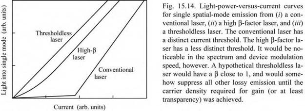
15.5 Thresholdless lasers There have been a number of papers describing a thresholdless laser as a possible communications device (De Martini et al., 1987). This would essentially be a light-emitting device that emitted most or all of its light into the fundamental spatial cavity mode. In this way, one can achieve the lasing condition of there being one photon in the cavity almost without gain. Let us denote the probability that light is emitted into the fundamental spatial cavity mode as p. If the в of the LED were almost 1, then the light-versus-current curve of the device would be linear, and indistinguishable from a laser with no threshold. A comparison of the light-versus-current for a conventional laser, a high-в laser, and a truly thresholdless laser is given in Fig. 15.14. If one envisions a thresholdless device as fabricated from a resonant-cavity pillar, there are a number of problems besides those of fabrication. Simply having a good sub-threshold intensity, giving only a small kink in the L-I curve between sub-threshold and lasing, is not good enough for a thresholdless laser. The output modulation of such a device would be extremely slow below threshold compared to the lasing regime. To enable lasing, there must be some gain, because the в will never be 1. For there to be gain, we must pump the active region past transparency first, since it is absorbing under no-pump conditions. This gain condition requires a certain carrier density, which, in fact, determines the threshold.
One can imagine a device such that all optical modes other than the fundamental are highly suppressed, and the internal quantum efficiency is nearly perfect. In this case, with even a small current, the carrier densities within the device would slowly build until the active region became transparent, and some light could get out through the fundamental optical mode. Such a device would have a very low threshold, but one would have to be careful not to ever drive the device below its threshold even momentarily, because of the long time required to build the necessary space charge inside the device for transparency. Also, if the fundamental emission was suppressed at low carrier densities, it is unlikely that the other modes would be suppressed by an even higher degree, which is what would be required not to lose the injected carriers. In fact, it is the difficulty in suppressing any side emission that makes semiconductor thresholdless lasers difficult if not impractical.
|
|
One could, of course, make a laser with a very small threshold by making the laser very small. The problem is that such a device would be capable of only a very small output power. For a hypothetical four-quantum-well single-mode LED, which does not rely on gain, but achieves a в close to 1, the current densities cannot be more than about 50 |j, A/^m2 or 5 kA/cm2. Using the formulas for в for a dielectric pillar (в > 0.5), and this current density, one can find that less than 2 ^.W could be emitted into a single mode for an RCLED pillar structure. This is clearly too small for high-speed communications in the 100-650 Mbit/s regime, where 10 ^.W is considered a minimum for an emitter. An RCLED with a very short carrier lifetime owing to extreme enhancement of the desired emission could have higher pump currents, but no semiconductor design can do this. If the device is a laser, higher powers could be drawn because of the reduced carrier lifetime, but the device sizes are incredibly small for real fabrication, or for any sort of heat dissipation.
In conclusion, semiconductor RCLEDs should remain devices larger than about 5 or 10 ^m in diameter, and should remain multimode emitters. Semiconductor vertical-cavity lasers are best fabricated at sizes that make sense technologically, without regard to the в factor of the spontaneous emission. A high-в laser may not be desirable anyway, since the spontaneous emission will introduce excess noise into the emission.
15.6 Other RCLED devices It is likely that the future of resonant-cavity LEDs and confined-photon emitters will involve new materials and applications from those currently used in communications and display systems. Spontaneously emitting confined-photon devices will always have competition from lasers, conventional LEDs, and other forms of devices. It is only a matter of time, however, before the right materials combination at the right wavelengths, for the right application, will make commercial devices a reality. It is therefore worthwhile to mention other confined photonic LED material systems.
Wilkinson et al. (1995) fabricated an AlGaAs/GaAs thin-film emitter with metal mirrors on a Si substrate, emitting at 880 nm. Pavesi et al. (1996) fabricated porous silicon RCLEDs at 750 nm wavelength. Fisher et al., (1995) investigated a conjugate polymer RCLED designed for 650 nm. Hadji et al. (1995) have realized CdHgTe/HgTe RCLEDs operating at a wavelength of 3.2 цш.
A structure of particular note is a GaAs/AlxOy RCLED (Huffaker et al., 1995) operating at 950 nm, where the aluminum oxide in the output mirror was produced from AlAs by oxidation. This composition of output mirror allows the effective cavity length to remain small, maximizing the output enhancement in the RCLED. The back mirror of the structure was Ag. Another particularly interesting device is the broadly tunable RCLED by Larson and Harris (1995). The top mirror is a deformable membrane which can be moved by electrostatic forces. Tunable emission was shown from 938 to 970 nm.


 Опубликовано в