Polarization effects in III-V nitrides
 1 апреля, 2014
  admin
admin The most common epitaxial growth direction of III-V nitrides is the с-plane of the hexagonal wurtzite structure. III-V nitrides grown on the с-plane have polarization charges located at each of the two surfaces of a layer. As a result of these charges, internal electric fields occur in III-V nitrides that have a significant effect on the optical and electrical properties of this class of semiconductors.
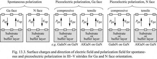
There are spontaneous polarization charges as well as strain-induced or piezoelectric polarization charges (Bernardini et al., 1997; Ambacher et al., 1999; 2000; 2002). The direction of the internal electric field depends on the strain and the growth orientation (Ga face or N face) and is shown for different cases in Fig. 13.3.
The strain in the epitaxial layer can be compressive or tensile. In the compressive-strain case, the epitaxial layer of interest is laterally compressed (“laterally” meaning “in the plane of the wafer”). For example, GaInN is compressively strained when grown on a thick relaxed GaN buffer layer. In the tensile-strain case, the epitaxial layer of interest is expanded along the lateral direction. For example, AlGaN is under tensile strain when grown on a thick relaxed GaN buffer layer.
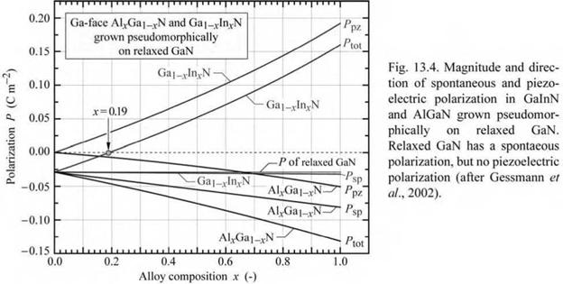
The calculated magnitude of the electric field for common III-V nitride alloys grown on
|
|
|
|
|
relaxed GaN is shown in Fig. 13.4 (Gessmann et al., 2002). |
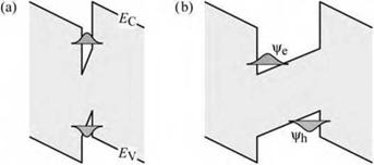
A consequence of the polarization fields for quantum well structures is shown in Fig. 13.5. The quantum well layers have an internal electric field that spatially separates electrons and holes thereby preventing efficient radiative recombination. This is particularly true for thick quantum wells, e. g. > 100 A. To avoid this deleterious effect, it is imperative that the quantum well layers are kept very thin. Quantum well thicknesses of 20-30 A are typically used to minimize such electron-hole separation effects.
The large electric fields caused by the polarization effects can be screened by a high free-
carrier concentration, which can be attained through either (i) high doping of the active region or (if) a high injection current. Screening of the internal electric field also results in a blue-shift of the emission, frequently found in GaInN LEDs as the injection current is increased.
|
|
Fig. 13.5. Schematic band diagram of (a) thin and (b) thick AlGaN/GaN active regions with polarization fields for Ga-face growth (substrate on right-hand side).
Polarization effects can be used advantageously to reduce ohmic contact resistances in GaN devices. Polarization-enhanced contacts to p-type GaN employ a thin, compressively strained GaInN cap layer that is deposited on the p-type GaN. The electric field in the GaInN cap layer is polarized in such a way that the tunneling probability of holes is enhanced (Li et al., 2000; Gessmann et al., 2002). Contact resistances as low as 1.1 x 10⁻⁶ and 2 x 10⁻⁷ Q cm2 have been reported for non-annealed and annealed polarization-enhanced ohmic contacts to p-type GaN, respectively (Kumakura et al., 2001; 2003). Both the concept of polarization-enhanced contacts and the very low specific contact resistances are remarkable because they represent a several orders-of-magnitude improvement over conventional contact technologies. The forward voltage of GaN-based LEDs with polarization-enhanced contacts is generally lower than the forward voltage of LEDs with conventional GaN contacts (Su, 2005).


 Опубликовано в